State monitoring and fault diagnosis method for large-scale semiconductor manufacture process

A technology for manufacturing process and fault diagnosis, applied in the direction of semiconductor/solid state device testing/measurement, etc., can solve the problem of not implementing process variable data set redundant information elimination, inability to effectively detect nonlinearity and multimodality, and inability to local variance information. Carry out effective extraction and other problems to achieve the effect of improving engineering applicability, avoiding difficult collection, and improving product quality and production efficiency

Inactive Publication Date: 2013-08-28
SHANGHAI UNIV
View PDF4 Cites 1 Cited by
  • Summary
  • Abstract
  • Description
  • Claims
  • Application Information

AI Technical Summary

Problems solved by technology

This method has the following deficiencies: [1] There is no effective elimination of redundant information in the process variable data set due to the large-scale process data set caused by the collected batch-manufacturing multi-sensing signals; [2] The feature extraction stage uses the principal element The analysis method can only extract the characteristics of the global variance information in the data set, but cannot effectively extract the local variance information, and may lose important information; [3] The spatial distribution of variable data in the semiconductor manufacturing process is usually nonlinear and multimodal , therefore, the SPE statistical index proposed based on the premise that the given data set should conform to the Gaussian distribution is usually unable to effectively detect nonlinear and multi-modal manufacturing process anomalies; [4] this method only monitors semiconductor manufacturing process anomalies , without identifying the cause of the process abnormality, that is, the failure diagnosis of the manufacturing process cannot be carried out

Method used


Image

  • State monitoring and fault diagnosis method for large-scale semiconductor manufacture process

Examples


Embodiment 1

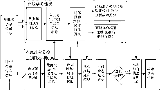
[0018] Such as figure 1 As shown, the state monitoring and fault diagnosis method of this large-scale semiconductor manufacturing process, the specific operation steps are as follows:

[0019] 1. Arrange relevant sensors at key positions in the semiconductor manufacturing process to pick up various signals that can reflect the performance status of the semiconductor manufacturing process (such as gas flow pressure during wafer etching, RF power supply size, RF resistance, voltage, etc.), and the signals pass through the data The filter circuit and amplifier circuit on the acquisition card perform data acquisition, and the data acquisition card also converts the analog signal into a digital signal, and the data collected by the data acquisition card is transmitted to the computing terminal through the network for further data analysis and processing. Assume that the number of all sensors on the production line is , the acquisition time duration of each sensor signal in t...


PUM


Abstract

The invention relates to a state monitoring and fault diagnosis method for a large-scale semiconductor manufacture process. The method comprises the following operation steps of: (1) unpacking of multiple batches of process data: unpacking a three-dimensional data set (namely variable number, sampling time and production batch) into a two-dimensional data set; (2) elimination of redundant information in the data set; (3) characteristic extraction of the data set; (4) state modeling of a manufacture process based on a Gaussian mixture model; (5) state monitoring of the manufacture process; and(6) fault diagnosis of the manufacture process. According to the method disclosed by the invention, the state monitoring and fault diagnosis of the large-scale semiconductor manufacture process can be achieved, thereby the operation reliability of a semiconductor manufacture system and the quality of an output wafer are improved, and further the production and operation cost is reduced.

Description

technical field [0001] The present invention is a state monitoring and fault diagnosis method for a large-scale semiconductor manufacturing process, involving multi-sensing signal data conversion, large-scale process data set dimension reduction and important feature extraction, data probability density distribution space description modeling, process state monitoring And fault diagnosis, to realize the status monitoring and fault diagnosis of complex large-scale semiconductor manufacturing process. The invention belongs to the technical field of state monitoring and fault diagnosis of manufacturing process. Background technique [0002] At present, the semiconductor manufacturing system presents a development trend of high automation, high precision, high reliability, and high intelligence, emphasizing the controllability, reliability, and maintainability of the manufacturing process. The semiconductor manufacturing process is quite complicated. The manufacturing process n...

Claims


Application Information

Patent Timeline
Patent Type & Authority Patents(China)
IPC IPC(8): H01L21/66
Inventor 余建波尹纪庭刘美芳
Owner SHANGHAI UNIV
Why Eureka
Try Eureka