Supercharge Your Innovation With Domain-Expert AI Agents!

LED (light emitting diode) encapsulation structure

A technology of light-emitting diodes and packaging structures, applied in electrical components, circuits, semiconductor devices, etc., can solve problems such as poor heat dissipation performance of chips, and achieve the effects of shortening heat dissipation paths, reducing thermal resistance, and extending service life

Inactive Publication Date: 2012-03-07
SHENZHEN REFOND OPTOELECTRONICS +1
View PDF7 Cites 3 Cited by
  • Summary
  • Abstract
  • Description
  • Claims
  • Application Information

AI Technical Summary

Problems solved by technology

[0003] The invention provides a light-emitting diode packaging structure, aiming to solve the problem of poor heat dissipation performance of the chip in the existing light-emitting diode packaging structure

Method used


Image

  • LED (light emitting diode) encapsulation structure
  • LED (light emitting diode) encapsulation structure
  • LED (light emitting diode) encapsulation structure

Examples


Embodiment Construction

[0008] In order to make the object, technical solution and advantages of the present invention clearer, the present invention will be further described in detail below in conjunction with the accompanying drawings and embodiments. It should be understood that the specific embodiments described here are only used to explain the present invention, not to limit the present invention.

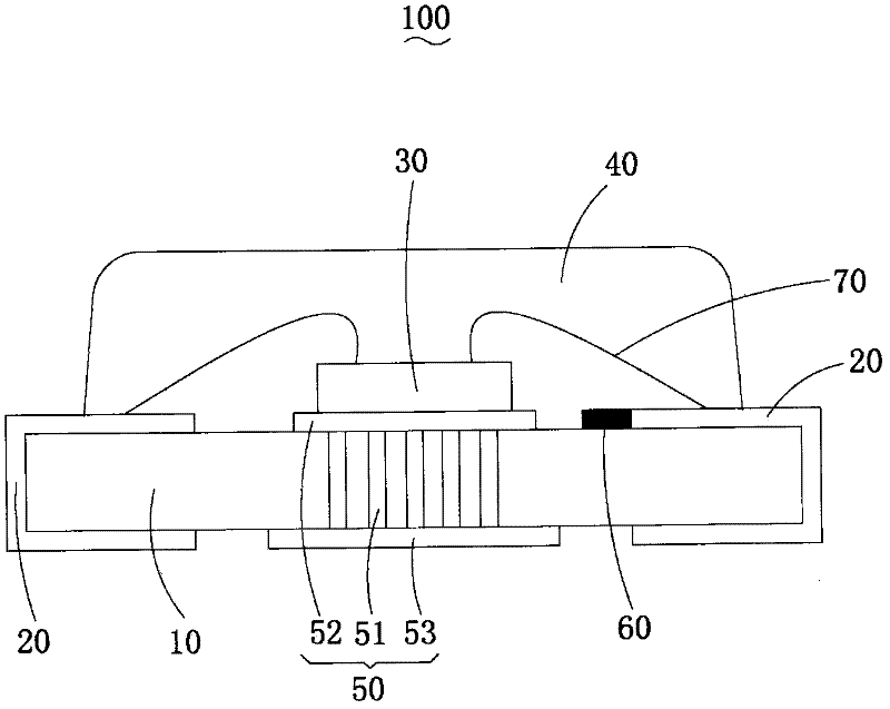
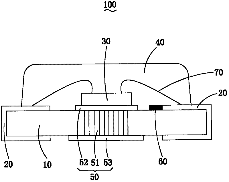
[0009] see figure 1 The light-emitting diode package structure 100 provided by the embodiment of the present invention includes a substrate 10, two pins 20 located on opposite sides of the substrate 10, a chip 30 seated on the substrate 10 and connected to the pins 20 by wire bonding , an encapsulation 40 packaged on the substrate 10 and covering the chip 30 , and a heat dissipation structure 50 passing through the substrate 10 to conduct the heat emitted by the chip 30 to the outside of the substrate 10 .

[0010] The pins 20 are metal pins, and are electrically connected with the chip 30 through...


PUM


Abstract

The invention provides an LED (light emitting diode) encapsulation structure which comprises a substrate, two pins, a chip and a cover, wherein the two pins are located on the two opposite sides of the substrate, the chip is arranged on the substrate and connected with the pins through wire bonding, and the cover is encapsulated on the substrate and covers the chip. The LED encapsulation structure also comprises a radiating structure which penetrates through the substrate and transfers the heat emitted by the chip to the outside of the substrate. The heat generated by the chip is transferred to the outside of the substrate through the radiating structure instead of the original mode of leading out the heat from the pins on the two sides, the radiating path is shortened, the thermal resistance is reduced, and the service life of an LED is prolonged.

Description

technical field [0001] The invention relates to a light-emitting element, in particular to a light-emitting diode packaging structure. Background technique [0002] At present, the package sizes of light-emitting diodes on the market are mainly 0603 (that is, the length and width are 1.6mm and 0.8mm), 0805 (that is, the length and width are 2.0mm and 1.25mm), and 1206 (that is, the length and width are 3.2mm). and 1.6mm), the selected PCB board is BT (Bismaleimide Triazine) board, and the thermal conductivity of BT board is low. When the light-emitting diode is working, the light-emitting chip needs to emit heat, and the ordinary epoxy resin on the outer seal has limited thermal conductivity. The heat is mainly exported by the metal pins on both sides of the PCB, so that the heat conduction path becomes larger and the thermal resistance increases. 1. The rise of the junction temperature of the chip accelerates the aging of the light-emitting diode, resulting in a decrease i...

Claims


Application Information

Patent Timeline
Patent Type & Authority Applications(China)
IPC IPC(8): H01L33/48H01L33/64
Inventor 朱益明
Owner SHENZHEN REFOND OPTOELECTRONICS
Features
  • R&D
  • Intellectual Property
  • Life Sciences
  • Materials
  • Tech Scout
  • Unparalleled Data Quality
  • Higher Quality Content
  • 60% Fewer Hallucinations
Learn More