Junction barrier schottky having low forward voltage drop

A Schottky potential and Schottky barrier layer technology, applied in electrical components, circuits, semiconductor devices, etc., can solve the problems of low leakage current, affect the switching speed of the device, and cannot be fully considered, and achieve low positive The effect of voltage drop, optimization of electrical parameter characteristics, and high device switching speed

Inactive Publication Date: 2012-03-14
上海芯石微电子有限公司
View PDF8 Cites 7 Cited by
  • Summary
  • Abstract
  • Description
  • Claims
  • Application Information

AI Technical Summary

Problems solved by technology

[0003] (2) P-i-N diodes provide lower leakage current and higher reverse voltage, but during the switching process, a certain amount of stored charge is stored on the PN junction, which affects the switching speed of the device
That is to say, it is not possible to give full consideration to both the on-state performance and the off-state performance.

Method used


Image

  • Junction barrier schottky having low forward voltage drop
  • Junction barrier schottky having low forward voltage drop
  • Junction barrier schottky having low forward voltage drop

Examples


Embodiment Construction

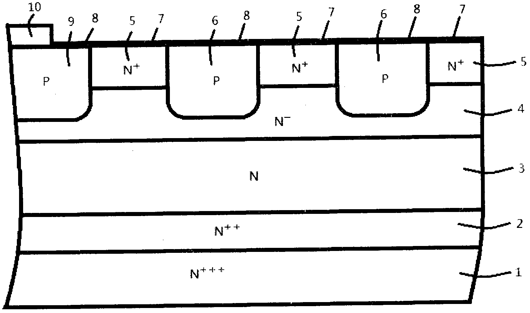
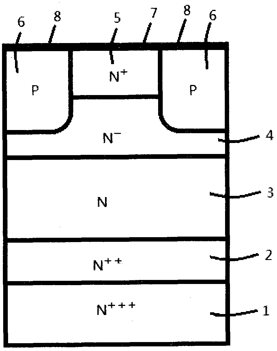
[0053] figure 1 Shows a schematic cross-sectional view of an embodiment of the present invention, the following combination figure 1 The semiconductor device of the present invention will be described in detail.

[0054] A semiconductor device includes: a substrate layer 1, which is an N conductivity type semiconductor material, and a cathode is drawn out through metal on the lower surface of the substrate layer; a buffer layer 2, which is located on the substrate layer 1, is an N conductivity type semiconductor material; and a drift layer 3, On the buffer layer 2, it is a semiconductor material of N conductivity type; the lightly doped layer 4 is on the drift layer 3, and the lightly doped layer is a semiconductor material of N conductivity; the heavily doped layer 5 is on the lightly doped layer Above 4 is a semiconductor material of the N conductivity type; the suppression zone 6 is a plurality of P-type regions formed separately from each other in the lightly doped layer and t...


PUM


Abstract

The invention discloses a novel junction barrier schottky device which comprises a substrate layer, a buffering layer, a drifting layer, a light doping layer, a plurality of restraining areas, a heavy doping layer and a schottky barrier layer, wherein the restraining areas which are separated from each other are located in the light doping layer and the heavy doping layer. When a reverse bias is applied to a semiconductor device, a large-area exhausting region is spread and formed in a semiconductor material of the light doping layer. The invention also provides a manufacturing method for the semiconductor device. The semiconductor device provided by the invention has a low forward voltage drop and a high device-switching speed. Electrical parameter characteristics of the semiconductor device are further optimized.

Description

Technical field [0001] The present invention mainly relates to the structure and manufacturing process of a junction barrier Schottky device, and in particular to a structure and manufacturing process of a new type of junction barrier Schottky device with low forward voltage drop. Background technique [0002] There are usually three types of rectifiers. (1) Schottky barrier diodes are devices that contact metal and semiconductors. They have low forward voltage drop and extremely high switching speed, but the reverse leakage current and reverse voltage are relatively large. The disadvantageous characteristics that are not high affect the applications within a certain range of the device. [0003] (2) P-i-N diodes provide lower leakage current and higher reverse voltage, but during the switching process, a certain amount of stored charge is stored on the PN junction, which affects the switching speed of the device. [0004] (3) Junction barrier Schottky diode is a Schottky structure ...

Claims


Application Information

Patent Timeline
Patent Type & Authority Applications(China)
IPC IPC(8): H01L29/872H01L29/06H01L29/36H01L21/329
CPCH01L29/872
Inventor 杨忠武
Owner 上海芯石微电子有限公司
Why Eureka
Try Eureka