High-efficiency Schottky rectifier and method of manufacturing same

a schottky rectifier, high-efficiency technology, applied in the direction of semiconductor devices, electrical apparatus, transistors, etc., can solve the problems of increasing the demand for low-voltage applications, high reverse leakage current of schottky barrier rectifiers, and inability to meet conventional trench schottky, etc., to achieve low forward voltage drop and high switching speed

Active Publication Date: 2010-05-04
DIODES INC
View PDF2 Cites 6 Cited by
  • Summary
  • Abstract
  • Description
  • Claims
  • Application Information

AI Technical Summary

Benefits of technology

[0006]The present invention provides a high-efficiency two-terminal semiconductor device comprising a Schottky barrier rectifier and a vertically-oriented JFET separated by a transition zone of inverted bias resulting from a three-layer epitaxial film, and a method of manufacturing the same. The device has use, for example, in high frequency, low-loss power circuit applications in which high switching speed and low forward voltage drop are desirable.
[0009]In one embodiment, the method of making the semiconductor device proceeds broadly as follows. Initially, the layers of the multi-layer epitaxial film are deposited in a single deposition process. During this process, the resistivity of one or more of the layers is established by introducing controlled amounts of n-type dopants in order to achieve desirable electrical characteristics for the layers. Alternatively, the desired resistivity profile can be established using subsequent diffusion processes. More specifically, the first layer is modified with an n-type dopant to provide a particular breakdown voltage; the second layer is modified with an n-type dopant to provide an area of reverse-direction electric field when the device is reverse-biased; and the third layer is modified with an n-type dopant to support and separate a first space charge region associated with an upper portion of the device and a second space charge region associated with the lower portion of the trench. The upper portion of the trench is etched into the multi-layer epitaxial film, and the first trench region is formed by associating an oxide with a surface of the upper portion of the trench. The lower portion of the trench is then etched, and the trench is substantially filled with the polysilicon doped with boron. The second trench region is formed by diffusing the boron into a surface of the lower portion of the trench. The device provides such desirable electrical characteristics as low forward voltage drop, low reverse current leakage, and very fast switching speed matching that of Schottky rectifiers and JFETs, while remaining a majority carrier device. The device, much like a JBS rectifier, eliminates the Schottky barrier lowering which occurs in standard Schottky rectifiers, but also reverses the direction of the electric field for the portion of the drift region of the diode under current blocking bias, which reduces the reverse leakage current more effectively than the JBS rectifier. Additionally, the device better utilizes chip surface area than MBS when designed for low voltage, low VF application.

Problems solved by technology

Unfortunately, Schottky barrier rectifiers suffer from undesirably high reverse leakage current when operating at elevated temperatures.
In addition to these high voltage applications, however, there is an increasing demand for low voltage applications, for which conventional trench Schottky is not well-suited.
Unfortunately, it also results in a significant reduction of the area available for the Schottky barrier because the trench may consume as much as 50% of the available area on a chip.

Method used


Image

  • High-efficiency Schottky rectifier and method of manufacturing same
  • High-efficiency Schottky rectifier and method of manufacturing same
  • High-efficiency Schottky rectifier and method of manufacturing same

Examples


Embodiment Construction

, below.

BRIEF DESCRIPTION OF THE DRAWINGS

[0011]A preferred embodiment of the present invention is described in detail below with reference to the attached drawing figures, wherein:

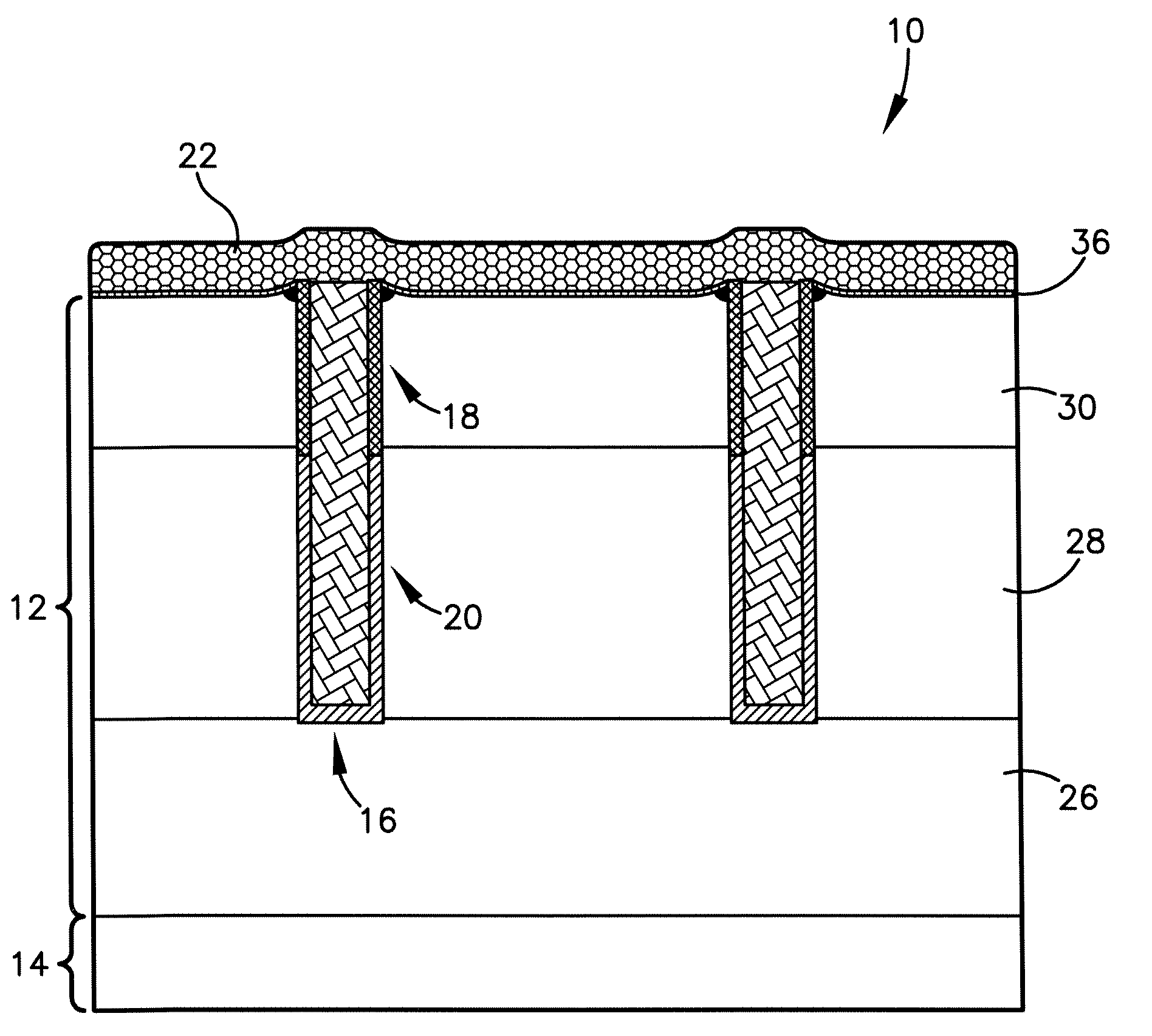
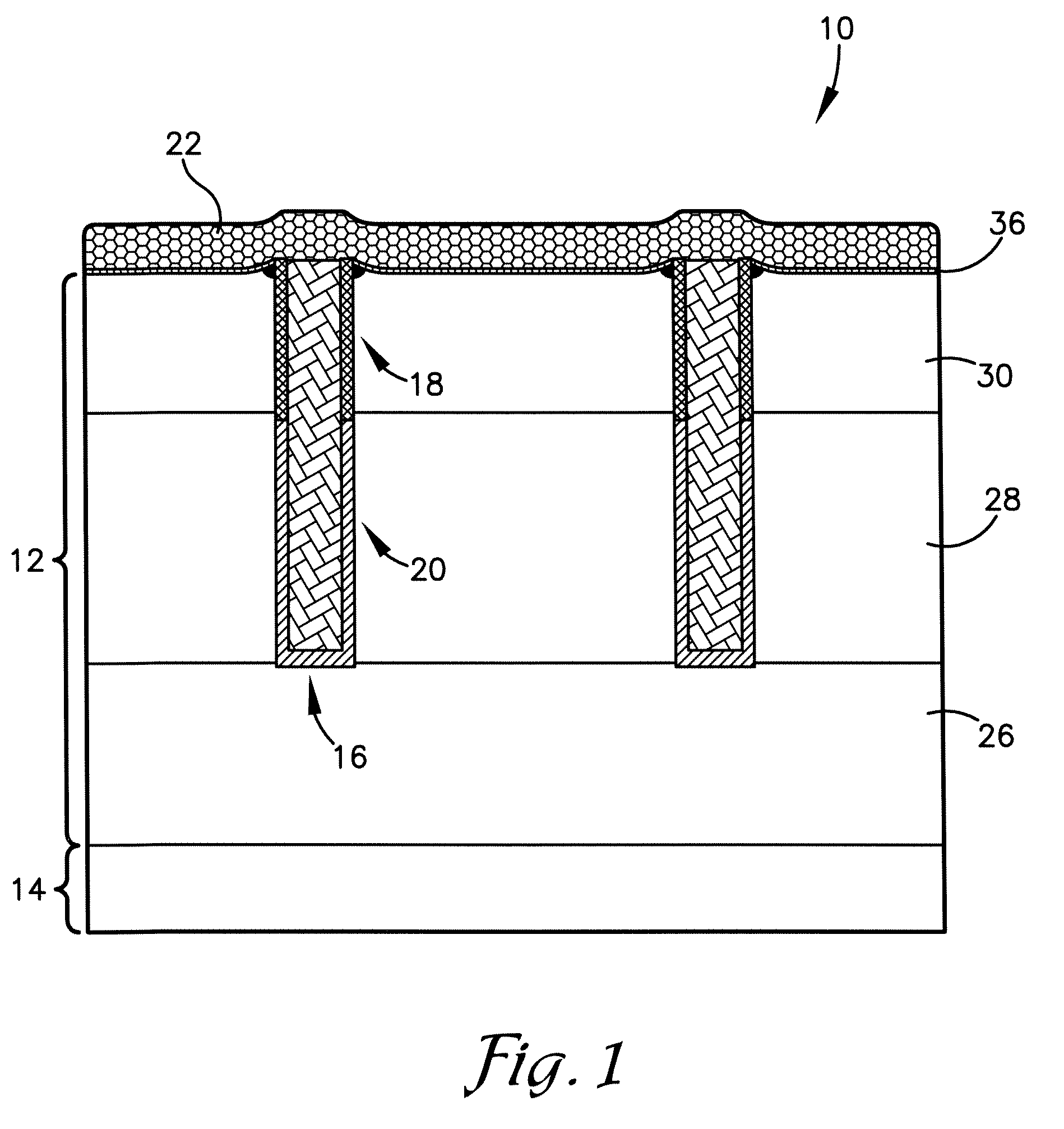
[0012]FIG. 1 is a cross-sectional elevation view of an embodiment of the device of the present invention;

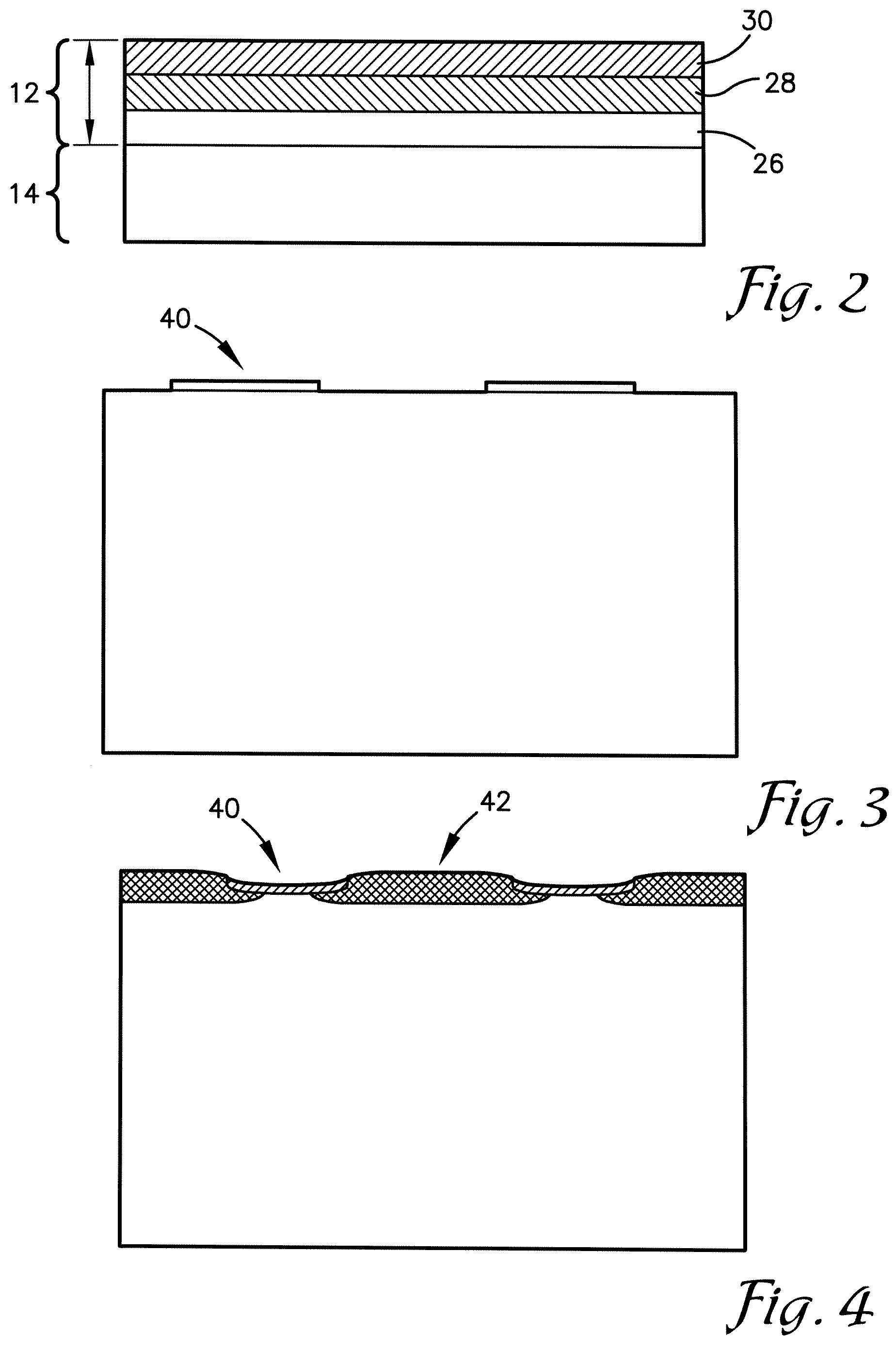
[0013]FIG. 2 is a cross-sectional elevation view of the device following an initial in a method of making the device of FIG. 1, showing a multi-layer epitaxial film having been deposited on a substrate;

[0014]FIG. 3 is a cross-sectional elevation view following a fourth step in the method, showing a deposit of nitride;

[0015]FIG. 4 is a cross-sectional elevation view following a fifth step in the method, showing a layer of oxide;

[0016]FIG. 5 is a cross-sectional elevation view following a sixth step in the method, showing the nitride of FIG. 3 removed;

[0017]FIG. 6 is a cross-sectional elevation view following a seventh step in the method, showing an implantation of boron;

[0018]FIG. 7 is a cross-sectional ...


PUM


Abstract

A rectifier device (10) comprising a multi-layer epitaxial film (12) and a rectifier and a transistor manufactured in the film (12), wherein the transistor is oriented vertically relative to the plane of the rectifier. The rectifier and transistor are separated by a transition zone of inverted bias. The rectifier is a Schottky barrier rectifier, and the transistor is a JFET. More specifically, the device (1) comprises the film (12), a trench (16), a first region (18) associated with an upper portion of the trench (16), and second region (20) associated with a lower portion. The interface between the p+ material of the second region (20) and the n material of the film (12) creates a p+ / n junction. The device (10) has use in high frequency, low-loss power circuit applications in which high switching speed and low forward voltage drop are desirable.

Description

FIELD OF THE INVENTION[0001]The present invention relates broadly to semiconductor rectifier devices, especially Schottky rectifiers, and methods of manufacturing the same. More specifically, the present invention concerns a two-terminal semiconductor rectifier device comprising an integrated Schottky barrier rectifier and vertically-oriented junction field effect transistor (JFET) separated by a transition zone of inverted bias resulting from a three-layer epitaxial film, and a method of manufacturing the same.BACKGROUND OF THE INVENTION[0002]Modern power circuits require power rectifiers with improved power switching performance. For some applications, p+ / n rectifiers with high switching speeds are used. High switching speeds are necessary to minimize reverse current flow during recovery. Majority carrier devices, such as Schottky barrier rectifiers, are often used because they offer both improved switching speed and lower forward voltage drop. Unfortunately, Schottky barrier rect...

Claims


Application Information

Patent Timeline
Patent Type & Authority Patents(United States)
IPC IPC(8): H01L29/80
CPCH01L29/0657H01L29/872H01L29/66143
Inventor HAMERSKI, ROMANHRUSKA, CHRISHOSSAIN, FAZIA
Owner DIODES INC
Why Eureka
Try Eureka