Semiconductor device

A semiconductor and device technology, applied in the field of structure and manufacturing process of junction barrier Schottky devices, can solve the problems of low forward voltage drop switching speed, affecting the switching speed of devices, and not being able to take full account of the problems, so as to reduce the positive voltage drop. The effect of the voltage drop, the optimization of electrical parameter characteristics, and the compact structure

Active Publication Date: 2012-08-08
HANGZHOU LION MICROELECTRONICS CO LTD
View PDF0 Cites 0 Cited by
  • Summary
  • Abstract
  • Description
  • Claims
  • Application Information

AI Technical Summary

Problems solved by technology

[0002] There are usually three kinds of rectifiers, (1) Schottky barrier diode, which is a metal and semiconductor contact device, has a low forward voltage drop and a very high switching speed, but has a large reverse leakage current and a reverse voltage Not high unfavorable characteristics affect the application of the device within a certain range
[0003] (2) P-i-N diodes provide lower leakage current and higher reverse voltage, but during the switching process, a certain amount of stored charge is stored on the PN junction, which affects the switching speed of the device
That is to say, it is not possible to give full consideration to both the on-state performance and the off-state performance.

Method used


Image

  • Semiconductor device
  • Semiconductor device
  • Semiconductor device

Examples


Embodiment 1

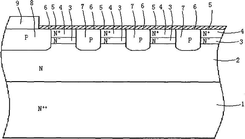
[0031] figure 1 Shows a schematic cross-sectional view of the first example of the semiconductor device of the present invention, combined below figure 1 The semiconductor device of the present invention will be described in detail.

[0032] A semiconductor device includes: a substrate layer 1, which is an N conductivity type semiconductor material, and a cathode is drawn out through a metal on the lower surface of the substrate layer; a drift layer 2, located on the substrate layer 1, is an N conductivity type semiconductor material; a depletion layer 3 , located on the drift layer 2, the depletion layer is an N-conduction type semiconductor material; the heavily doped layer 4 is located on the depletion layer, and is an N-conduction type semiconductor material; the reverse bias leakage current suppression structure region 7 is multi The P-type regions are separately formed in the drift layer, the depletion layer and the heavily doped layer, and each anti-bias leakage curren...

Embodiment 2

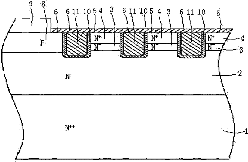
[0038] figure 2 Shown is a schematic cross-sectional view of the second embodiment of the semiconductor device of the present invention, combined below figure 2 Detailed description.

[0039] Other structures are as in Embodiment 1, a plurality of separated reverse bias leakage current suppression structure regions 7 are formed in the drift layer 2, depletion layer 3 and heavily doped layer 4, and the reverse bias leakage current suppression structure region 7 is a trench structure , including a trench insulating layer 10 and polysilicon 11 filled in the trench insulating layer 10 , the width of each reverse bias leakage current suppression structure region 7 is 2-6um, and the distance between each other is 2-10um.

[0040]A drift layer 2, a depletion layer 3 and a heavily doped layer 4 are formed on the substrate layer 1 by means of epitaxial production, and the phosphorus impurity concentration in the drift layer is set to, for example, 2×10 15 Atom / CM 3 , the phosphoru...


PUM


Abstract

The invention discloses a semiconductor device which comprises a substrate layer, a drifting layer, a depletion layer, suppression back biased leakage current structure areas, a heavily doped layer and a schottky barrier layer, wherein a plurality of mutually separated suppression back biased leakage current structure areas are positioned in the shifting layer, the depletion layer and the heavy doped layer and used for expanding in the semiconductor material of the depletion layer to form a large-area depletion area when back bias voltage is applied to the semiconductor device. The invention also provides a manufacture method of the semiconductor device. The semiconductor device and the manufacture method can reduce a certain quantity of reverse leakage current while reducing a certain quantity of forward voltage drop, has simple structure and process and low manufacture cost, improves the switching speed of the device and further optimizes the electrical parameter property of the device.

Description

technical field [0001] The present invention mainly relates to the structure and manufacturing process of a junction barrier Schottky device, in particular to the structure and manufacturing process of a novel junction barrier Schottky device with low forward voltage drop and low reverse leakage current at the same time . Background technique [0002] There are usually three kinds of rectifiers, (1) Schottky barrier diode, which is a metal and semiconductor contact device, has a low forward voltage drop and a very high switching speed, but has a large reverse leakage current and a reverse voltage The unfavorable characteristics that are not high affect the application of the device within a certain range. [0003] (2) P-i-N diodes provide lower leakage current and higher reverse voltage, but during the switching process, a certain amount of stored charge is stored on the PN junction, which affects the switching speed of the device. [0004] (3) Junction barrier controlled ...

Claims


Application Information

Patent Timeline
Patent Type & Authority Patents(China)
IPC IPC(8): H01L29/872H01L21/329H01L27/06H01L21/82
Inventor 朱江
Owner HANGZHOU LION MICROELECTRONICS CO LTD
Why Eureka
Try Eureka