Semiconductor power device with ultralow power consumption and preparation method

A power device and ultra-low power consumption technology, which is applied in the field of ultra-low power semiconductor power devices and their preparation, can solve problems such as low withstand voltage, complex device structure and process, and increased process levels, and achieve low forward voltage drop , save area, and reduce the cost of tape-out

Inactive Publication Date: 2016-08-24
ZHANGJIAGANG CASS SEMICON
View PDF5 Cites 7 Cited by
  • Summary
  • Abstract
  • Description
  • Claims
  • Application Information

AI Technical Summary

Problems solved by technology

However, the fly in the ointment is that due to the introduction of the field plate structure of the shielded gate in the device structure, the device structure and process are more complicated, resulting in an increase in process levels. At present, it is mainly realized by 7-layer photolithography process.
Moreover, the shielded gate is connected to the source on the terminal guard ring, and the electric field is mainly concentrated inside the first guard ring near the cell area during the reverse withstand voltage, resulting in a low withstand voltage

Method used


Image

  • Semiconductor power device with ultralow power consumption and preparation method
  • Semiconductor power device with ultralow power consumption and preparation method
  • Semiconductor power device with ultralow power consumption and preparation method

Examples


Embodiment Construction

[0035]First, combined with the Figure 18 , taking an N-channel structure as an example to describe in detail a specific implementation of an ultra-low power consumption semiconductor power device of the present invention.

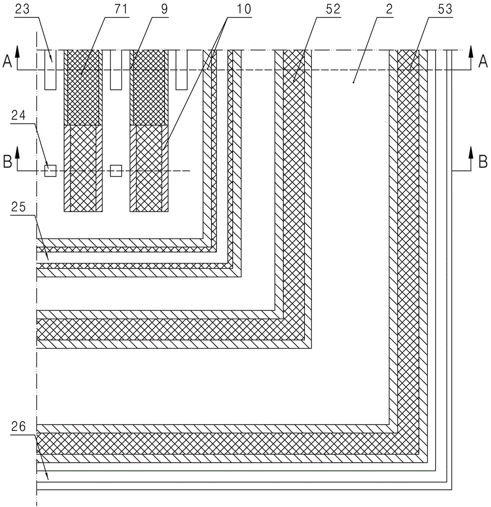
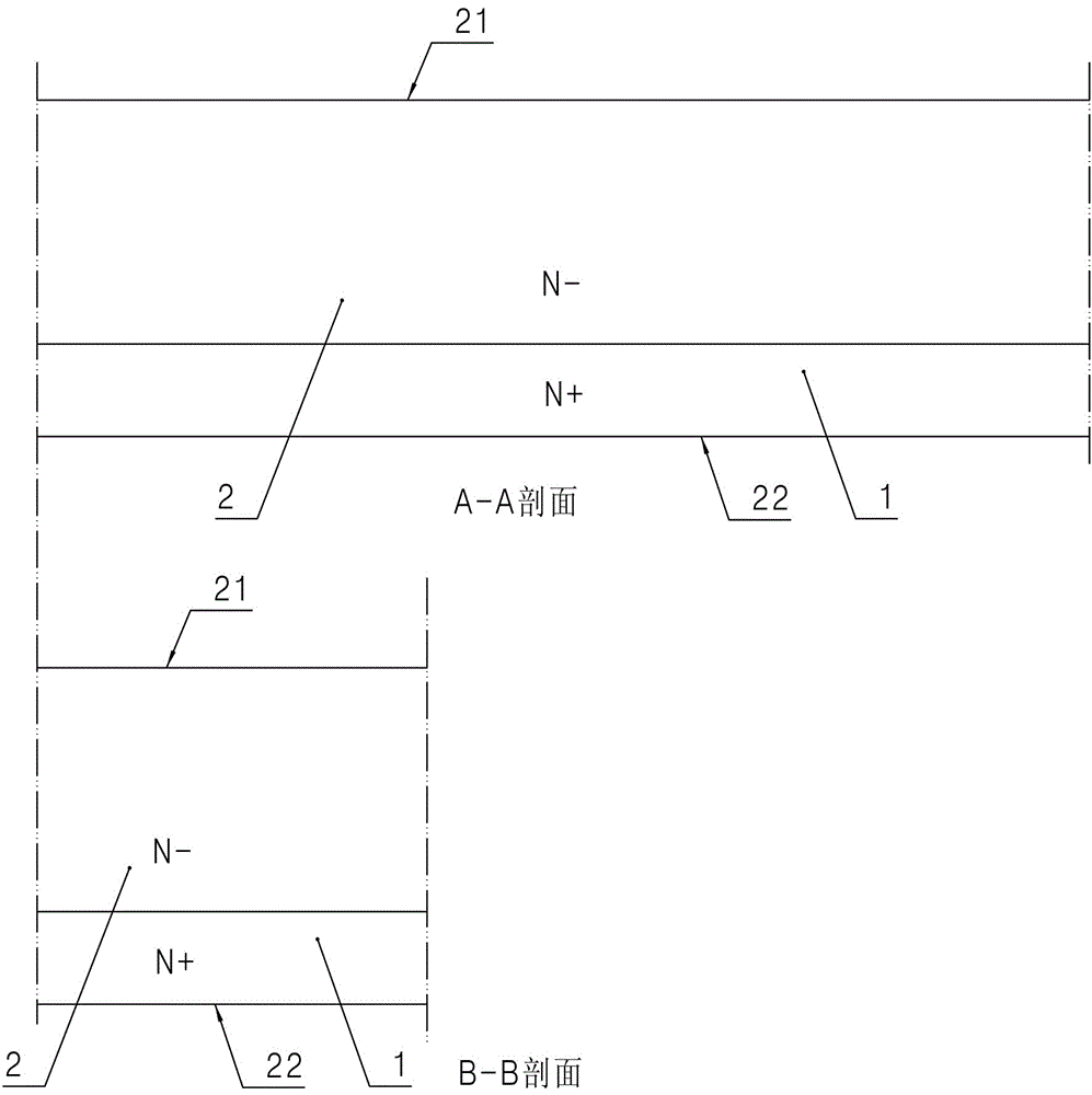
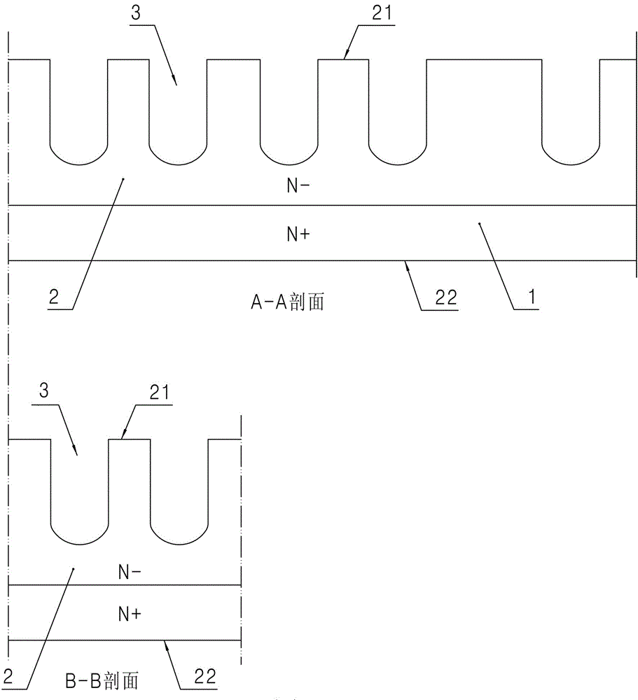
[0036] Such as Figure 18 As shown, a kind of ultra-low power consumption semiconductor power device described in the present invention comprises: semiconductor substrate, and semiconductor substrate comprises: N-type substrate 1 (also referred to as N+ substrate) and be arranged on N-type substrate 1 N-type epitaxial layer 2 (also called N- epitaxial layer), the surface of N-type epitaxial layer 2 is the first main surface 21, and the surface of N-type substrate 1 is the second main surface 22—see figure 2 As shown; the first main surface 21 includes: a cell area provided with cells and a terminal protection area located on the periphery of the cell area;

[0037] The specific structure of the cell includes: the first groove 3 set in the cell area, tha...


PUM


Abstract

The invention discloses a semiconductor power device with ultralow power consumption, wherein the quantity of photo-etching layers is small, and reverse recovery time is short. The device comprises a semiconductor baseplate, wherein a cellular area and a terminal protection area are disposed on the semiconductor base plate; and cells are disposed in the cellular area. The structure of the cellular area comprises a cellular groove, wherein upper conductive polycrystalline silicon layers and lower conductive polycrystalline silicon layers are disposed in the cellular groove; two sides of the upper conductive polycrystalline silicon layers are symmetrically disposed at extension parts which are located on two sides of the lower conductive polycrystalline silicon layers so as to form a cap-shaped structure. At least two voltage partition rings and at least one stop ring are disposed in the terminal protection area. The conductive polycrystalline silicon layer close to a voltage partition groove of the cellular area is electrically connected to a source electrode of the device; the rest conductive polycrystalline silicon layers in the voltage partition groove are suspended; and a Schottky diode is disposed in a transition area which is located between the cellular area and the terminal protection area. The invention also discloses a method which can be used for manufacture of the semiconductor power device with the ultralow power consumption.

Description

technical field [0001] The invention relates to a semiconductor power device and a preparation method thereof, in particular to an ultra-low power consumption semiconductor power device and a preparation method thereof. Background technique [0002] The current ultra-low power semiconductor power device is the same as the ordinary semiconductor power device. It has a parasitic diode connected in parallel with it. The anode of the parasitic diode is connected to the body and source of the power device, and the cathode is connected to the drain of the power device. Therefore, power devices are often used for freewheeling and clamping voltage. During freewheeling or clamping voltage, the parasitic diode is forward-conducting, and the power device is also conducting. The source (anode of the parasitic diode) voltage of the power device is higher than the drain ( The cathode of the parasitic diode) has a slightly higher voltage, and the current flows from the source to the drain;...

Claims


Application Information

Patent Timeline
Patent Type & Authority Applications(China)
IPC IPC(8): H01L29/06H01L29/423H01L29/78H01L21/027H01L21/28H01L21/336
CPCH01L21/0274H01L29/0623H01L29/4236H01L29/42376H01L29/66484H01L29/66666H01L29/7827H01L29/7831
Inventor 侯宏伟丁磊
Owner ZHANGJIAGANG CASS SEMICON
Why Eureka
Try Eureka