

Preparation method of power diode
A power diode, N-type technology, used in semiconductor/solid-state device manufacturing, electrical components, circuits, etc., can solve the problem of high cost
- Summary
- Abstract
- Description
- Claims
- Application Information
AI Technical Summary
Problems solved by technology
Method used
Image

Examples
Embodiment Construction
[0018] In order to make the objects, features and advantages of the present invention more comprehensible, specific implementations of the present invention will be described in detail below in conjunction with the accompanying drawings.
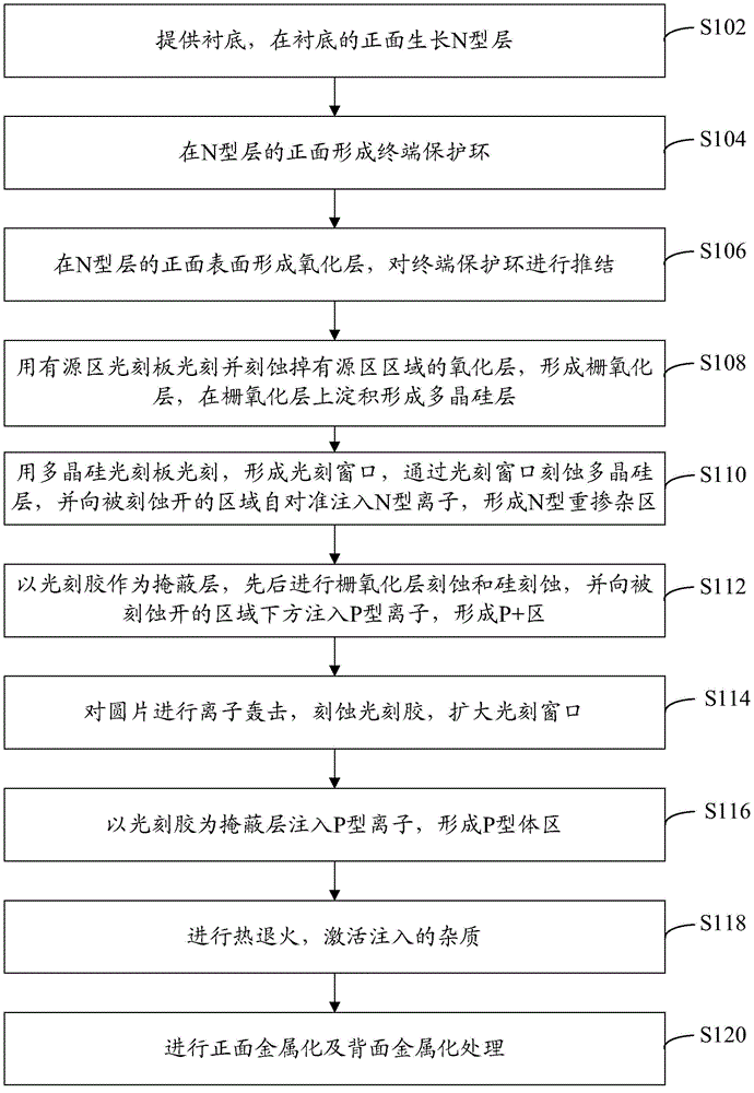
[0019] Such as figure 1 Shown is a flow chart of a method for preparing a power diode according to an embodiment. The preparation method includes the following steps.
[0020] Step S102, providing a substrate, and growing an N-type layer on the front surface of the substrate.
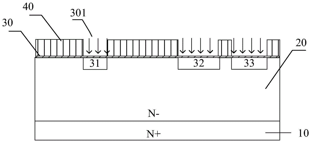
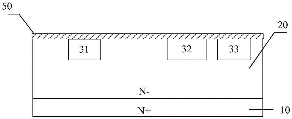
[0021] The material of the substrate 10 may be semiconductor materials such as silicon, silicon carbide, gallium arsenide, indium phosphide, or silicon germanium. In this embodiment, the substrate 10 is an N-type silicon wafer with crystal orientation .
[0022] In this embodiment, an N-type layer 20 with a certain thickness and resistivity is epitaxially grown on the front side of the substrate 10 (the side where the front side structure of the power diode is form...
PUM
| Property | Measurement | Unit |
|---|---|---|
| Thickness | aaaaa | aaaaa |
| Thickness | aaaaa | aaaaa |
Abstract
Description
Claims
Application Information