Method for manufacturing 50A high-current fast recovery diode

A technology for recovering diodes and manufacturing methods, which is applied in the manufacture of circuits, electrical components, semiconductors/solid-state devices, etc., and can solve poor environmental adaptability such as poor PN junction passivation effect, temperature shock resistance, and large reverse recovery time and other problems, to achieve the effect of improving high temperature working stability, high long-term working reliability, and increasing the reverse voltage range

Active Publication Date: 2015-01-07
西安卫光科技有限公司
View PDF3 Cites 9 Cited by
  • Summary
  • Abstract
  • Description
  • Claims
  • Application Information

AI Technical Summary

Problems solved by technology

[0004] At present, polyimide is generally used to passivate PN junction mesa at home and abroad. This process has the advantages of simple process, low cost, and large batch output. However, since polyimide is an organic polymer passivation material and has poor temperature stability, this process is used The PN junction passivation effect of the product of the technology is poor, the reverse leakage current is relatively large at high temperature, the product has poor environmental adaptability such as temperature shock resistance, and the stability of long-term work is not ideal
[0005] In actual use, it is also found that the high-current recovery diodes formed by the prior art still have the problems of low current (generally below 50A) and excessive reverse recovery time, which cannot meet the needs of high-current and high-frequency circuits.
[0006] Third, most of the high-current recovery diode packages formed by the existing technology are glass packages and plastic packages, which cannot be used in environments with high and low temperature changes, strong mechanical stress, and radiation in actual use.

Method used


Image

  • Method for manufacturing 50A high-current fast recovery diode
  • Method for manufacturing 50A high-current fast recovery diode
  • Method for manufacturing 50A high-current fast recovery diode

Examples


Embodiment Construction

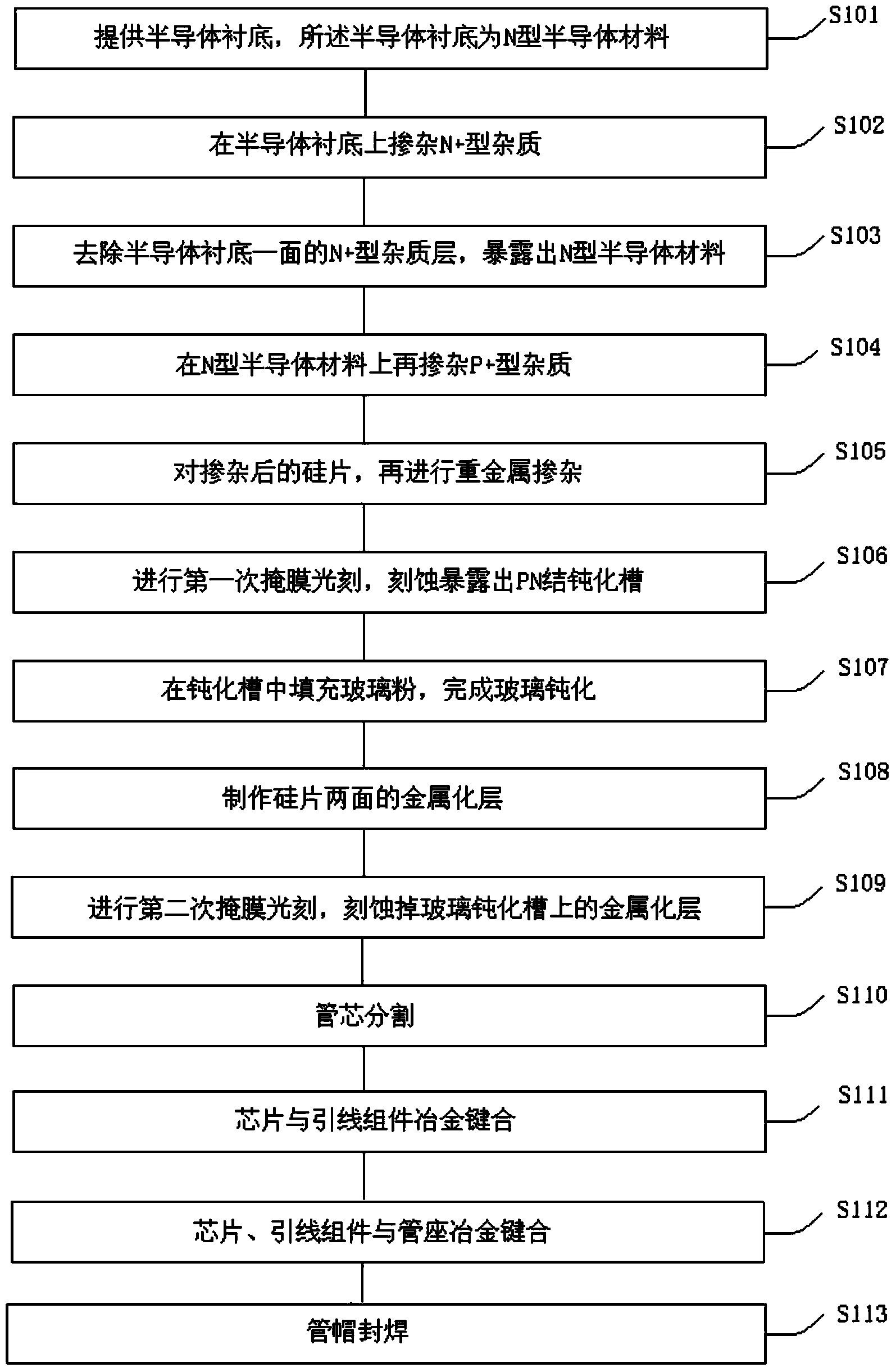
[0055] In order to make the object, technical solution and advantages of the present invention clearer, the implementation manner of the present invention will be further described in detail below in conjunction with the accompanying drawings.

[0056] combine figure 1 The flow chart of the present invention illustrates the method step of the present invention:

[0057] A manufacturing method of a 50A high-current fast recovery diode, comprising the steps of:

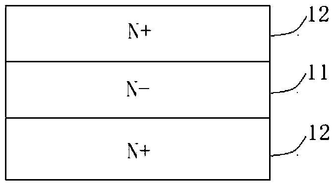
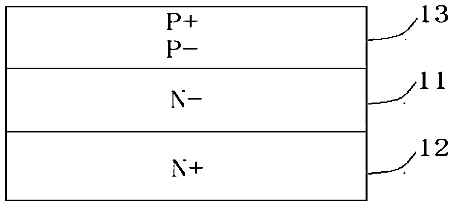
[0058] Step S101, providing a semiconductor substrate, the semiconductor substrate is an N-type semiconductor silicon material, and different material resistivities can be selected according to different reverse voltages; see figure 2 N-type silicon material layer 11.

[0059] Step S102, doping N on the N-type semiconductor substrate + Type impurities (compounds of phosphorus, such as P 2 o 5 or phosphine), which is generally achieved by high-temperature diffusion, and the diffusion temperature is between 1000°C a...


PUM


Abstract

The invention discloses a method for manufacturing a 50A high-current fast recovery diode. The method for manufacturing the 50A high-current fast recovery diode comprises the steps that an N type semiconductor silicon material is provided to serve as a semiconductor substrate; the N type semiconductor substrate is doped with N+ type impurities; the N+ type impurity layer on one side of the semiconductor substrate is removed; an exposed N-type semiconductor material is doped with dual P+ type impurities; heavy metal platinum doping is conducted according to the high-temperature diffusion method; primary mask photoetching is conducted; glass powder is arranged in a passivation groove through knife coating, high-temperature sinter molding is conducted, and then PN junction glass passivation is completed; multiple metallization layers are manufactured on the two sides of a silicon wafer according to the vacuum sputtering method; secondary mask photoetching is conducted; the silicon wafer is divided into independent dies; a chip and a lead component are bonded together; the chip, the lead component and a diode holder are bonded together in a metallurgical mode through sintering; a diode cap and the diode holder are welded together in a sealed mode through percussion welding. According to the method for manufacturing the 50A high-current fast recovery diode, the manufacturing process based on the method is less influenced by the environment, the technology is mature, the stability and the repeatability are high, and the method can be widely used for volume production of high-current fast recovery diodes.

Description

technical field [0001] The invention belongs to the technical field of semiconductors, and relates to a manufacturing method of a 50A high-current fast recovery diode. Background technique [0002] High-current fast-recovery diodes are widely used in the rectification of electronic circuits and power systems due to their large operating current (above 50A), small forward voltage (below 1.4V), and short reverse recovery time (100ns). In particular, high-power switching circuits are essential. [0003] Since all electronic circuits and power supply systems generate heat during operation, the high-temperature stability of electronic components in the circuit has become an important technical indicator for assessing product quality and reliability. The stability directly affects the stability of the output current, thus determining whether the circuit and power supply can work normally. The high-temperature stability of high-current fast-recovery diodes is mainly determined by...

Claims


Application Information

Patent Timeline
Patent Type & Authority Applications(China)
IPC IPC(8): H01L21/329
CPCH01L29/6609
Inventor 王嘉蓉
Owner 西安卫光科技有限公司
Why Eureka
Try Eureka