

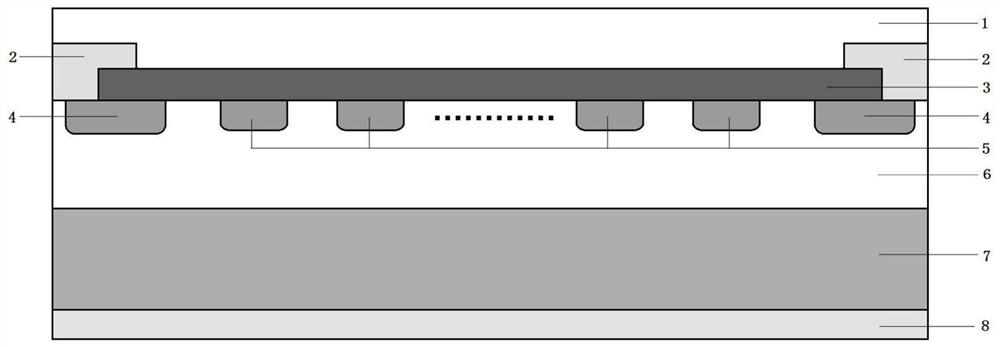
Gallium oxide junction barrier Schottky diode with field plate structure
A junction barrier Schottky and gallium oxide technology, which is applied in the field of gallium oxide junction barrier Schottky diodes, can solve the problems of uneven electric field of the device, increased leakage current, poor device reliability, etc., to improve the critical The breakdown field strength and breakdown voltage, the effect of alleviating the effect of electric field concentration, and reducing the reverse leakage current
- Summary
- Abstract
- Description
- Claims
- Application Information
AI Technical Summary
Problems solved by technology
Method used
Image

Examples
Embodiment 1
[0037] In Example 1, a gallium oxide junction barrier Schottky diode with a P-type annular material region and a P-type gate-shaped material region of P-type NiO and an anode field plate length of 1 μm was fabricated.
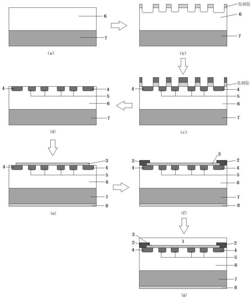
[0038] Step 1, for a thickness of 300 μm and a doping concentration of 10 18 cm -3The surface of the gallium oxide substrate is pretreated.
[0039] 1.1) The gallium oxide substrate was immersed in acetone solution, absolute ethanol solution and deionized water for ultrasonic cleaning for 10min each, and the cleaned gallium oxide substrate was blown dry with nitrogen gas;
[0040] 1.2) Place the cleaned and dried gallium oxide substrate in H 2 Thermal treatment was performed at a temperature of 1000°C in an atmospheric reaction chamber to remove surface contaminants.
[0041] Step 2, deposit a gallium oxide epitaxial layer, such as figure 2 a.
[0042] The pretreated gallium oxide substrate was put into the hydride vapor phase epitaxy deposition system, a...
Embodiment 2
[0063] In Example 2, a gallium oxide junction barrier Schottky diode with a P-type annular material region and a P-type gate-shaped material region of P-type GaN and an anode field plate length of 5 μm was fabricated.
[0064] Step 1, the thickness is 650μm, the doping concentration is 10 19 cm -3 The surface of the gallium oxide substrate is cleaned and pretreated.
[0065] The specific implementation of this step is the same as that of step 1 in Embodiment 1.
[0066] The second step is to grow a gallium oxide epitaxial layer, such as figure 2 a.
[0067] The pretreated gallium oxide substrate was put into the hydride vapor phase epitaxy deposition system, and the N 2 For carrier gas, keep the temperature at 1200K, N 2 The flow rate is 20.3slm, the flow rate of GaCl is 60slm, the proportion of GaCl is 0.05, the deposition thickness is 8 μm, and the doping concentration is 10 17 cm -3 gallium oxide epitaxial layer.
[0068] Step 3, making a P-type annular material re...
Embodiment 3
[0088] In Example 3, a gallium oxide junction barrier Schottky diode with the P-type annular material region and the P-type gate-shaped material region being P-type diamond and the anode field plate length of 10 μm was fabricated.
[0089] Step A, with a thickness of 450 μm and a doping concentration of 10 20 cm -3 The surface of the gallium oxide substrate is cleaned and pretreated.
[0090] The specific implementation of this step is the same as that of step 1 in Embodiment 1.
[0091] Step B, growing a gallium oxide epitaxial layer, such as figure 2 a.
[0092] The pretreated gallium oxide substrate was put into the hydride vapor phase epitaxy deposition system, and the N 2 For carrier gas, keep the temperature at 2000K, N2 The flow rate is 48slm, the GaCl flow rate is 100slm, the GaCl ratio is 0.5, the deposition thickness is 10μm, and the doping concentration is 10 18 cm -3 Gallium oxide epitaxial layer.
[0093] Step C, making the P-type annular material area and...
PUM
| Property | Measurement | Unit |
|---|---|---|
| length | aaaaa | aaaaa |
| thickness | aaaaa | aaaaa |
| thickness | aaaaa | aaaaa |
Abstract
Description
Claims
Application Information