Gallium oxide-based heterogeneous PN junction diode and preparation method thereof

A PN junction diode, gallium oxide-based technology, used in semiconductor/solid-state device manufacturing, electrical components, circuits, etc., can solve the problem of large reverse leakage current of unipolar Schottky barrier diodes, inability to prepare power devices, shock Low breakdown voltage and other problems, to achieve the effect of low reverse leakage current, stable performance and high withstand voltage

Inactive Publication Date: 2019-08-02
SUN YAT SEN UNIV
View PDF6 Cites 9 Cited by
  • Summary
  • Abstract
  • Description
  • Claims
  • Application Information

AI Technical Summary

Problems solved by technology

However, currently Ga 2 o 3 The p-type doping of materials has not yet been reliably realized, so it is impossible to prepare traditional power devices based on bipolar PN junction structures. Most of the existing gallium oxide-based diodes use unipolar Schottky barrier structures (see document K .Konishi, et al., 1-kV vertical Ga 2 o 3 field-plated Schottky barrier diodes, Applied Physics Letters 110(10), 103506, 2017 and Chinese patent CN 106876484A)
Compared with bipolar PN junction diode devices, unipolar Schottky barrier diodes have disadvantages such as large reverse leakage current, low breakdown voltage, and poor reliability. Therefore, how to realize gallium oxide-based PN junction diodes has become the current One of the key problems that the industry needs to solve urgently

Method used


Image

  • Gallium oxide-based heterogeneous PN junction diode and preparation method thereof
  • Gallium oxide-based heterogeneous PN junction diode and preparation method thereof

Examples


Embodiment Construction

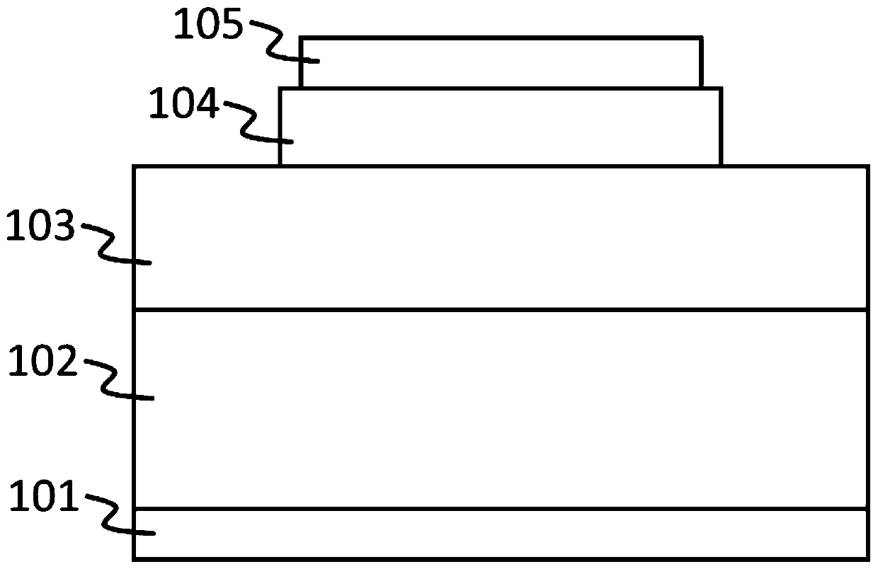
[0018] Such as figure 1 As shown, a gallium oxide-based heterogeneous PN junction diode described in the present invention includes a cathode electrode 101, an n-type doped gallium oxide substrate 102, and an n-type doped gallium oxide withstand voltage layer 103, which are sequentially stacked and connected, and also includes Anode electrode 105, p-type oxide semiconductor layer 104. One side of the p-type oxide semiconductor layer 104 is stacked and connected to the n-type doped gallium oxide withstand voltage layer 103, and the other side is stacked and connected to the anode electrode 105. The p-type oxide semiconductor layer 104 and the n-type doped The heterogallium oxide withstand voltage layer 103 forms a PN junction. The p-type oxide semiconductor layer 104 is an amorphous or polycrystalline structure with a hole concentration of 1×10 17 / cm 3 ~1×10 20 / cm 3 . The n-type doped gallium oxide withstand voltage layer 103 has a single crystal structure, and the dopi...


PUM

PropertyMeasurementUnit
thicknessaaaaaaaaaa
thicknessaaaaaaaaaa

Abstract

The invention discloses a gallium oxide-based heterogeneous PN junction diode and a preparation method thereof, and relates to the technical field of semiconductor devices. In allusion to the shortcomings such as high reverse leakage current, low breakdown voltage and poor reliability of gallium-oxide-based diodes in the prior art, it is proposed that a p-type oxide semiconductor layer is arrangedbetween an n-type doped gallium oxide voltage resistant layer and an anode electrode. The amorphous or polycrystalline p-type oxide semiconductor layer and the single crystal n-type doped gallium oxide voltage resistant layer are adopted to form a heterogeneous PN junction, the advantage of high hole concentration of the amorphous or polycrystalline p-type oxide semiconductor layer is utilized while giving full play to the high voltage resistant advantage of the single crystal gallium oxide material, and the p-type doping problem of the gallium oxide material is skillfully avoided. The realized diode device has the advantages of low reverse leakage current, high voltage resistance and stable performance, and the preparation process is simple.

Description

technical field [0001] The invention relates to the technical field of semiconductor devices, in particular to a gallium oxide-based heterogeneous PN junction diode and a preparation method thereof. Background technique [0002] Gallium oxide (Ga 2 o 3 ) semiconductor has an ultra-wide bandgap up to 4.8eV and an ultra-large breakdown field strength of 8MV / cm, and can produce large-size single crystal substrates by low-cost melting growth method, which is an ideal material for preparing ultra-high-power power electronic devices. However, currently Ga 2 o 3 The p-type doping of materials has not yet been reliably realized, so it is impossible to prepare traditional power devices based on bipolar PN junction structures. Most of the existing gallium oxide-based diodes use unipolar Schottky barrier structures (see document K .Konishi, et al., 1-kV vertical Ga 2 o 3 field-plated Schottky barrier diodes, Applied Physics Letters 110(10), 103506, 2017 and Chinese patent CN 106...

Claims


Application Information

Patent Timeline
Patent Type & Authority Applications(China)
IPC IPC(8): H01L29/861H01L29/267H01L29/06H01L21/34
CPCH01L29/0615H01L29/267H01L29/66969H01L29/8613
Inventor 卢星王钢裴艳丽陈梓敏
Owner SUN YAT SEN UNIV
Why Eureka
Try Eureka