Gallium oxide based hybrid PiN Schottky diode and preparation method thereof

A Schottky diode, gallium oxide technology, applied in semiconductor/solid-state device manufacturing, electrical components, circuits, etc., can solve the problems of low breakdown voltage, inapplicability, poor temperature characteristics of Schottky barrier diodes, etc. The effect of good pressure resistance

Active Publication Date: 2019-08-09
SUN YAT SEN UNIV
View PDF7 Cites 11 Cited by
  • Summary
  • Abstract
  • Description
  • Claims
  • Application Information

AI Technical Summary

Problems solved by technology

However, since there is no reliable method to achieve p-type doping of gallium oxide materials, the existing gallium oxide-based diodes mostly use Schottky barrier structures (see literature K.Konishi, et al., 1-kV vertical Ga2O3field-plated Schottky barrier diodes, AppliedPhysics Letters 110(10), 103506, 2017 and Chinese Patent CN 106876484A)
Compared with PN junction diodes, Schottky barrier diodes have low forward turn-on voltage and short reverse recovery time, but their reverse leakage current is large and breakdown voltage is low, and the temperature characteristics of Schottky barrier diodes are also relatively low. poor
[0003] Although some patent documents cover diodes made of p-type gallium oxide materials, they all have a single-anode structure and cannot achieve a dual-anode structure of mixed PiN.
At the same time, because the doping of P-type gallium oxide is very difficult, and the current technology cannot achieve a high enough doping concentration, it is not suitable for normal device use at all.

Method used


Image

  • Gallium oxide based hybrid PiN Schottky diode and preparation method thereof
  • Gallium oxide based hybrid PiN Schottky diode and preparation method thereof
  • Gallium oxide based hybrid PiN Schottky diode and preparation method thereof

Examples


Embodiment Construction

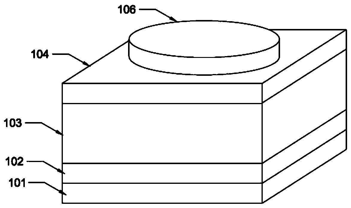
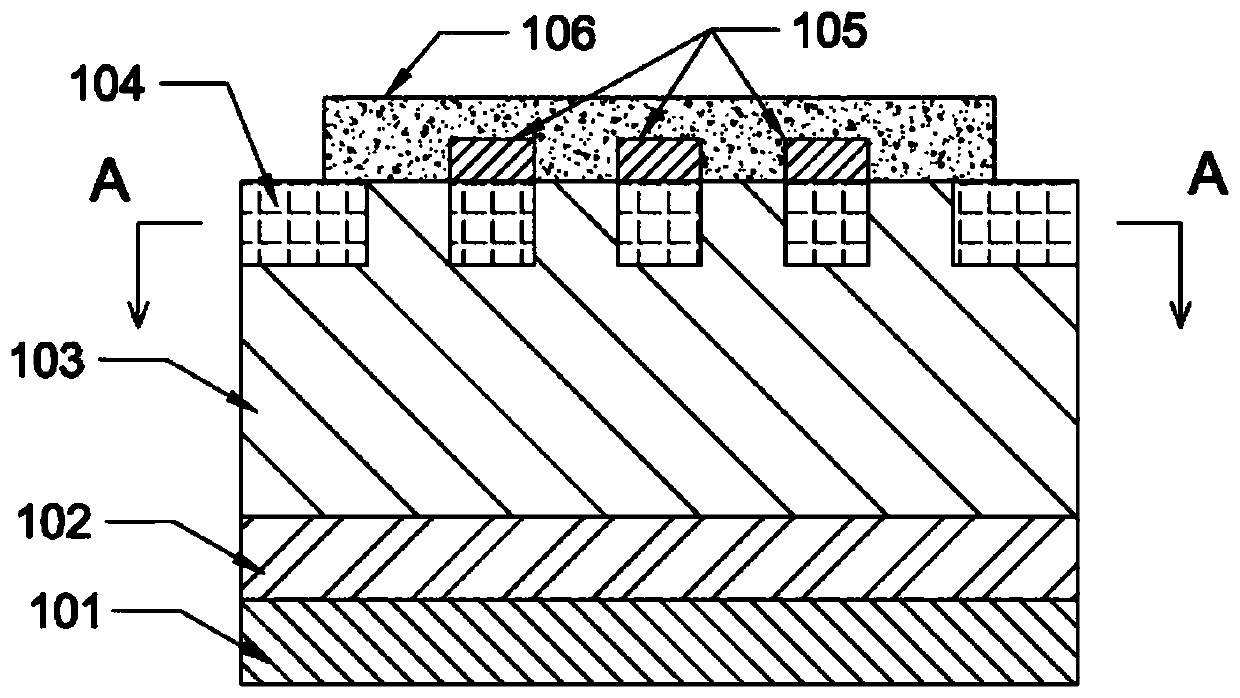
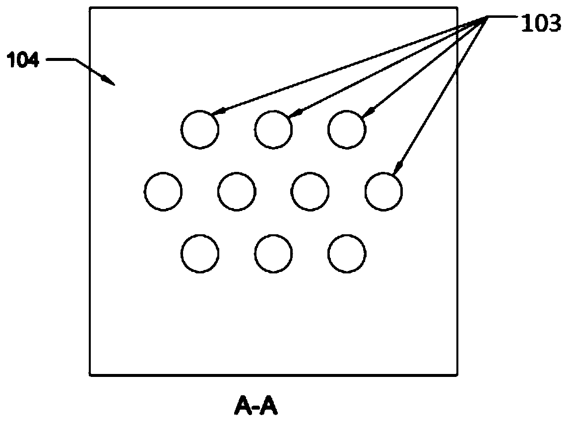
[0022] Such as Figure 1-3 As shown, a cathode electrode 101, an n-type doped gallium oxide substrate 102, a gallium oxide withstand voltage layer 103, and a p-type oxide semiconductor layer are sequentially stacked in a gallium oxide-based mixed PiN Schottky diode according to the present invention. 104 and the anode layer, the side of the gallium oxide withstand voltage layer 103 close to the p-type oxide semiconductor layer 104 is provided with a number of steps extending through the p-type oxide semiconductor layer 104, and the steps penetrate the p-type oxide semiconductor layer Layer 104 is then in contact with the anode layer; the step between the anode layer and the gallium oxide withstand voltage layer 103 is a Schottky contact; the anode layer and the p-type oxide semiconductor layer 104 are Schottky or ohmic touch. The n-type doped gallium oxide substrate 102 and the cathode electrode 101 are in ohmic contact. The anode layer includes a first anode electrode 105 a...


PUM


Abstract

The invention discloses a gallium oxide based hybrid PiN Schottky diode and a preparation method thereof, and relates to the technical field of semiconductor devices. The P-type gallium oxide in the prior art is very difficult to dope, and a sufficiently high doping concentration cannot be achieved in the prior art such that the diode in the prior art cannot adapt to a normal device. A diode of ahybrid PiN Schottky structure achieved by using a method of inserting a p-type oxide semiconductor layer into the surface of a gallium oxide voltage-resistant layer is provided. The method ingeniouslyavoids the p-type doping of a gallium oxide material. The reverse breakdown voltage and leakage current of the diode are both determined by a heterogeneous PN junction. Thus, a good voltage withstandcharacteristic is achieved while a good forward turn-on characteristic is achieved.

Description

technical field [0001] The invention relates to the technical field of semiconductor devices, in particular to a gallium oxide-based mixed PiN Schottky diode and a preparation method thereof. Background technique [0002] Rectifier diodes are widely used in switching power supplies, frequency converters, drives and other circuits. Gallium oxide (Ga 2 o 3 ) semiconductor has an ultra-wide bandgap up to 4.8eV and an ultra-large breakdown field strength of 8MV / cm, and can produce large-size single crystal substrates by low-cost melting growth method, which is an ideal material for preparing high-power rectifier diodes. However, since there is no reliable method to achieve p-type doping of gallium oxide materials, the existing gallium oxide-based diodes mostly use Schottky barrier structures (see literature K.Konishi, et al., 1-kV vertical Ga2O3field-plated Schottky barrier diodes, Applied Physics Letters 110(10), 103506, 2017 and Chinese patent CN 106876484A). Compared with...

Claims


Application Information

Patent Timeline
Patent Type & Authority Applications(China)
IPC IPC(8): H01L29/06H01L29/24H01L29/861H01L29/872H01L21/34
CPCH01L29/0684H01L29/24H01L29/247H01L29/66969H01L29/8613H01L29/872
Inventor 卢星王钢裴艳丽陈梓敏
Owner SUN YAT SEN UNIV
Why Eureka
Try Eureka