Gallium oxide vertical junction field effect transistor and preparation method thereof

A field effect transistor, vertical junction technology, applied in transistors, semiconductor/solid-state device manufacturing, semiconductor devices, etc., can solve the problems of poor gate control characteristics and difficult gate dielectric preparation, and achieve guaranteed gate control characteristics and good gate control characteristics. The effect of control characteristics and simple preparation process

Active Publication Date: 2020-05-01
SUN YAT SEN UNIV
View PDF4 Cites 0 Cited by
  • Summary
  • Abstract
  • Description
  • Claims
  • Application Information

AI Technical Summary

Problems solved by technology

However, since there is no reliable way to achieve p-type doping of gallium oxide materials, the existing vertical field effect transistors of gallium oxide all use metal-oxide-semiconductor (MOS) structure gates, see the literature Z.Hu, et al. ,Enhancement-mode Ga2O3Vertical Transistors with Breakdown Voltage>1kV,IEEE Electron Device Letters 39(6),869-872,2018; and CN108493234A, there are disadvantages such as difficult gate dielectric preparation and poor gate control characteristics

Method used


Image

  • Gallium oxide vertical junction field effect transistor and preparation method thereof
  • Gallium oxide vertical junction field effect transistor and preparation method thereof

Examples


Embodiment Construction

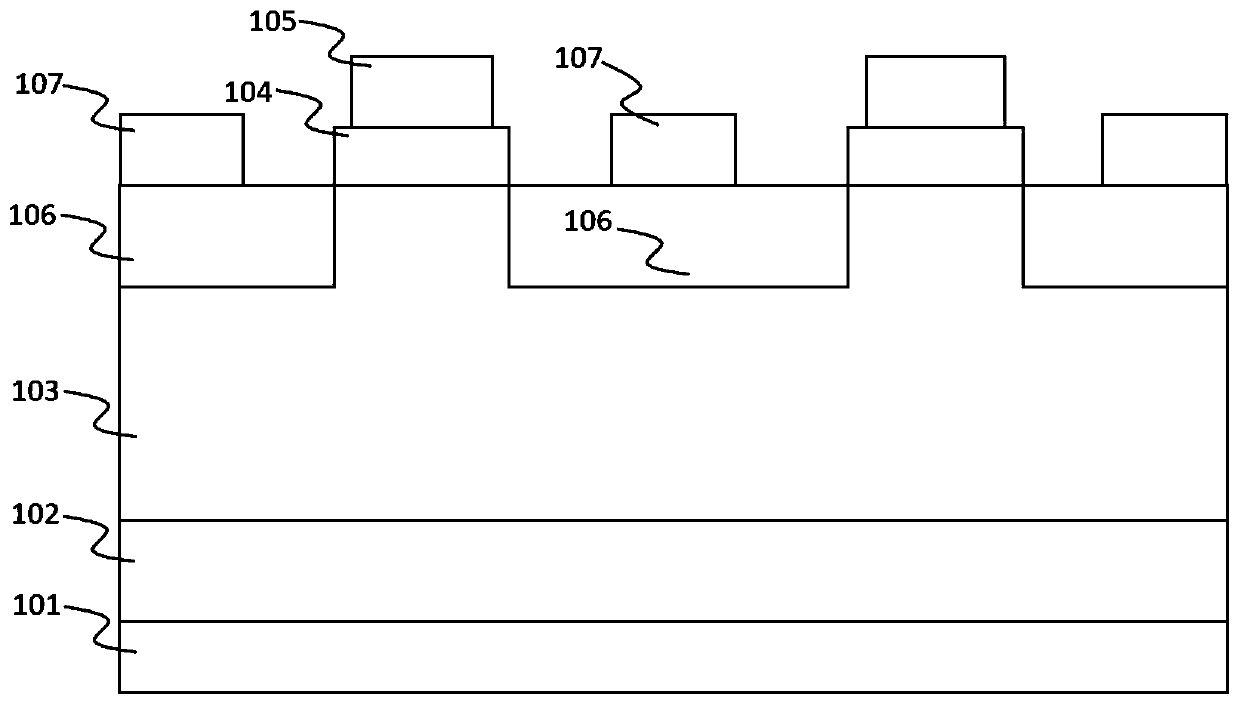
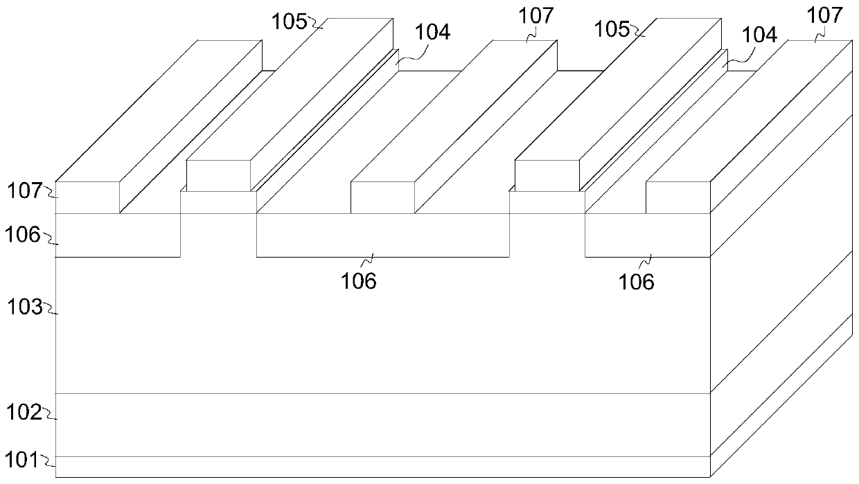
[0018] Such as figure 1 , 2 As shown, a gallium oxide vertical junction field effect transistor according to the present invention includes: a gallium oxide drift layer 103, an n-type doped gallium oxide substrate 102 and a drain electrode 101 which are sequentially stacked. The gallium oxide drift layer 103 extends outward from the side of the n-type doped gallium oxide substrate 102, and the ribs are stacked in order to provide gallium oxide contacts in the direction away from the n-type doped gallium oxide substrate 102. Layer 104 and source electrode 105. Both sides of the ribs are filled with a p-type oxide semiconductor layer 106, and the surface of the p-type oxide semiconductor layer 106 is provided with a gate electrode 107. The p-type oxide semiconductor layer 106 and the gate electrode 107 are in Schottky contact or ohmic contact; the drain electrode 101 is in ohmic contact with the surface of the n-type doped gallium oxide substrate 102; the source electrode 105 is ...


PUM

PropertyMeasurementUnit
thicknessaaaaaaaaaa
heightaaaaaaaaaa
thicknessaaaaaaaaaa

Abstract

The invention discloses a gallium oxide vertical junction field effect transistor and a preparation method thereof, and relates to the technical field of semiconductor devices. The scheme is proposedin view of the deficiencies such as difficult p-type doping of gallium oxide, high difficulty of gate dielectric preparation and poor gate control property in the prior art. Two sides of a three-dimensional fin channel structure are filled with a p-type oxide semiconductor layer to form a heterogeneous PN junction, so that the problem of p-type doping of the gallium oxide material is skillfully avoided, the good gate control property is ensured, and the preparation process is simple.

Description

Technical field [0001] The invention relates to the technical field of semiconductor devices, in particular to a gallium oxide vertical junction field effect transistor and a preparation method thereof. Background technique [0002] Gallium oxide (Ga 2 O 3 ) The semiconductor has an ultra-wide band gap of up to 4.8eV and an ultra-large breakdown field strength of 8MV / cm, and a large-size single crystal substrate can be prepared by a low-cost melt growth method, which is the preparation of ultra-high-power vertical field effect transistors (FET) Ideal material for devices. However, since there is no reliable method to achieve p-type doping of gallium oxide materials, the current existing gallium oxide vertical field-effect transistors all use metal-oxide-semiconductor (MOS) structure gates, see literature Z.Hu, etal. ,Enhancement-mode Ga2O3Vertical Transistors with Breakdown Voltage> 1kV, IEEE Electron Device Letters 39(6), 869-872, 2018; and CN108493234A, which have disadvant...

Claims


Application Information

Patent Timeline
Patent Type & Authority Patents(China)
IPC IPC(8): H01L29/10H01L29/80H01L21/337
CPCH01L29/1066H01L29/66893H01L29/802
Inventor 卢星王钢裴艳丽陈梓敏
Owner SUN YAT SEN UNIV
Why Eureka
Try Eureka