

Method for manufacturing silicon carbide semiconductor device
a semiconductor device and silicon carbide technology, applied in the direction of semiconductor devices, basic electric elements, electrical appliances, etc., can solve the problems of large reverse leakage current, low contact resistance, and schottky barrier diodes, and achieve low reverse leakage current, high forward current, and low resistance
- Summary
- Abstract
- Description
- Claims
- Application Information
AI Technical Summary
Benefits of technology
Problems solved by technology
Method used
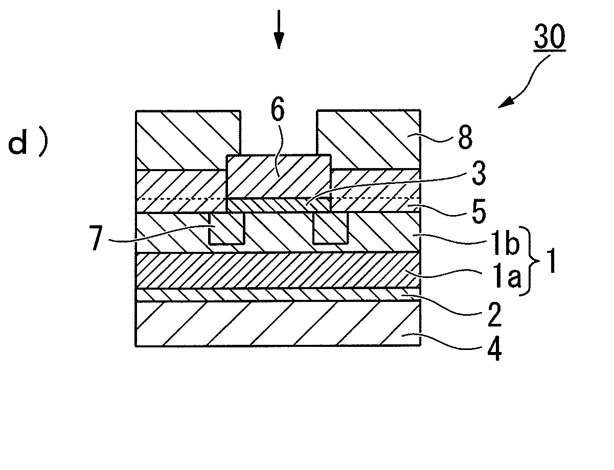
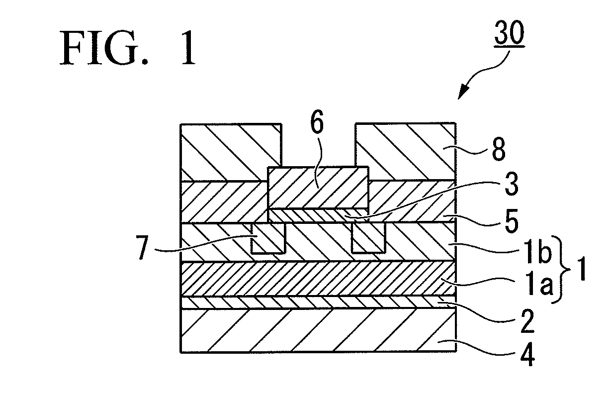
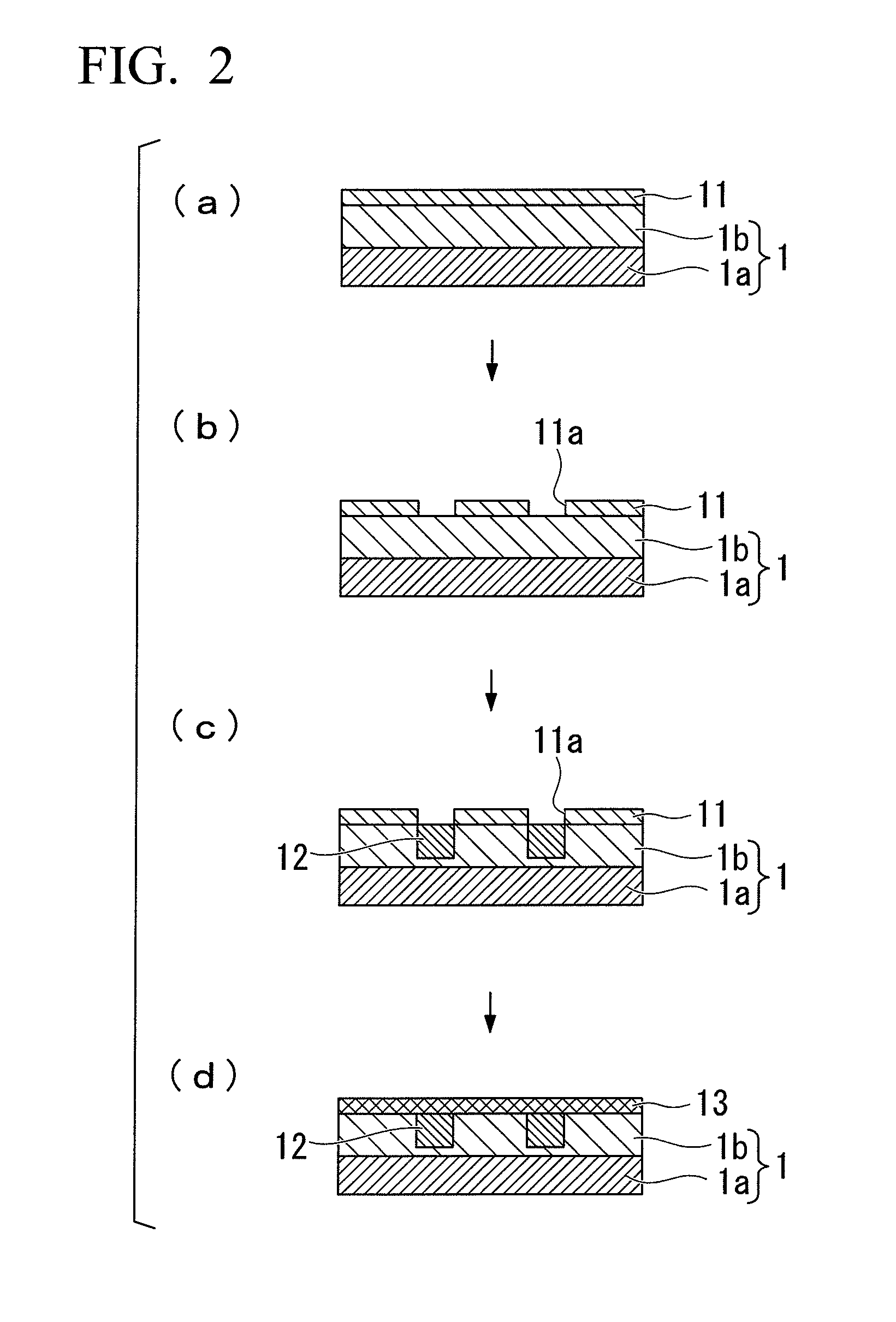
Image

Examples
example 1
[0071]A Schottky barrier diode of the example was manufactured by the following procedure.
[0072]First, as a SiC semiconductor, an n-type 4H—SiC semiconductor layer was prepared which was epitaxially grown to a thickness of 8 μm and at a carrier concentration of 1×1016 cm−3, on an n-type 4H—SiC semiconductor substrate (its thickness was 350 μm and its resistivity was 0.02 Ωcm) having a diameter of 3 inches.
[0073]Next, the surface of the above-mentioned SiC semiconductor was cleaned, and then was heated in an oxygen atmosphere at 1,200° C. for 2 hours, to form a thermal oxide film. Thereafter, a resist film was applied to the n-type 4H—SiC semiconductor epitaxial layer side, and the thermal oxide film on the 4H—SiC semiconductor substrate side was removed by immersion in HF for 10 minutes. The resist film was removed by immersion in an organic solvent. In this way, the thermal oxide film was formed only on the n-type 4H—SiC semiconductor epitaxial layer side.
[0074]Ne...
example 2
[0079]A Schottky bather diode of the example was manufactured by the following procedure.
[0080]First, as a SiC semiconductor, an n-type 4H—SiC semiconductor layer was prepared which was epitaxially grown to a thickness of 8 μm and at a carrier concentration of 1×1016 cm−3, on an n-type 4H—SiC semiconductor substrate (its thickness was 350 μm and its resistivity was 0.02 Ωcm) having a diameter of 3 inches.
[0081]Next, the surface of the above-mentioned SiC semiconductor was cleaned, and then was heated in an oxygen atmosphere at 1,200° C. for 2 hours, to form a thermal oxide film. Thereafter, a resist film was applied to the n-type 4H—SiC semiconductor epitaxial layer side, and the thermal oxide film on the 4H—SiC semiconductor substrate side was removed by immersion in HF for 10 minutes. The resist film was removed by immersion in an organic solvent. In this way, the thermal oxide film was formed only on the n-type 4H—SiC semiconductor epitaxial layer side.
[0082]Nex...
PUM
| Property | Measurement | Unit |
|---|---|---|
| temperature | aaaaa | aaaaa |
| temperature | aaaaa | aaaaa |
| thickness | aaaaa | aaaaa |
Abstract
Description
Claims
Application Information