PN junction base coupled gallium nitride Schottky diode and production method thereof

A Gallium Nitride Schottky and base coupling technology, which is applied in the direction of diode, semiconductor/solid-state device manufacturing, electrical components, etc., can solve the problems affecting the forward characteristics of the device, affecting the reliability of the device, reducing the device current, etc., to achieve Low cost, reduced electric field strength, improved breakdown voltage and reverse breakdown voltage

Pending Publication Date: 2022-01-21
西安电子科技大学广州研究院 +1
View PDF0 Cites 2 Cited by
  • Summary
  • Abstract
  • Description
  • Claims
  • Application Information

AI Technical Summary

Problems solved by technology

Edge termination is an effective method to suppress electrode edge electric field crowding and solve the problem of premature breakdown of quasi-vertical Schottky diodes. However, edge termination at the anode affects the forward characteristics of the device, increasing the on-resistance and reducing the device current. In addition It may also induce deep level traps in the GaN drift layer, affecting the reliability of the device

Method used


Image

  • PN junction base coupled gallium nitride Schottky diode and production method thereof
  • PN junction base coupled gallium nitride Schottky diode and production method thereof
  • PN junction base coupled gallium nitride Schottky diode and production method thereof

Examples


Embodiment 1

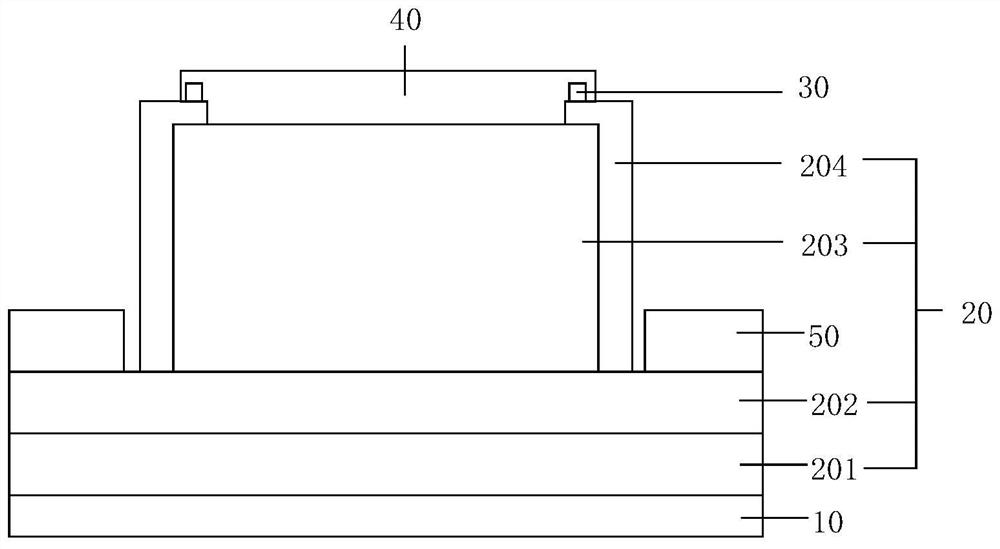
[0037] See figure 1 , figure 1 A schematic structural diagram of a gallium nitride Schottky diode coupled to a PN junction base provided by an embodiment of the present invention. The PN junction base-coupled GaN Schottky diode is a high-voltage Schottky diode, which includes a substrate layer 10 , an epitaxial layer 20 , an ohmic electrode 30 , an anode 40 and a cathode 50 .

[0038] Wherein, the epitaxial layer 20 is located on the substrate layer 10 . The epitaxial layer 20 is a Group-III nitride epitaxial layer, including a buffer layer 201, a contact layer 202, a drift layer 203, and a regrowth barrier layer 204. The buffer layer 201, the contact layer 202, and the drift layer 203 are stacked sequentially from bottom to top, and the regrowth potential The barrier layer 204 is arranged on the side surface and part of the upper surface of the drift layer 203, and a PN junction is formed between the regrowth barrier layer 204 and the drift layer 203; the ohmic electrode 30...

Embodiment 2

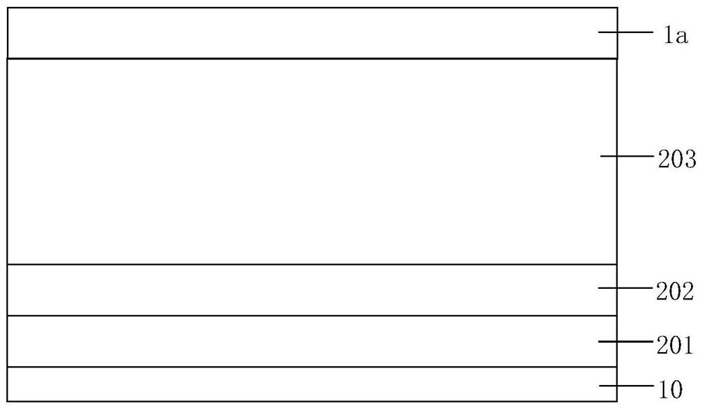
[0052] On the basis of Example 1, please refer to Figure 2a-Figure 2j , Figure 2a-Figure 2j It is a process schematic diagram of a method for manufacturing a PN junction base-coupled high-voltage gallium nitride Schottky diode provided by an embodiment of the present invention. The preparation method comprises steps:

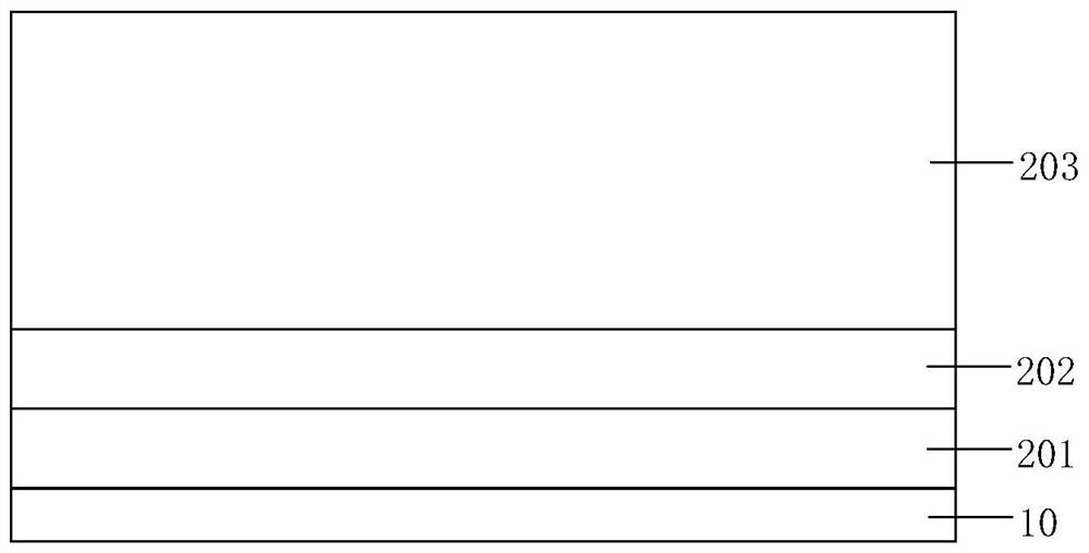
[0053] S1. Epitaxially grow the buffer layer 201, the contact layer 202 and the drift layer 203 on the substrate layer 10 in sequence, please refer to Figure 2a .

[0054] In this embodiment, the buffer layer 201 is an AlN / GaN superlattice buffer layer with a thickness of 750 nm; the contact layer 202 is a heavily doped N-type contact layer with a thickness of 1 μm and a doping concentration of 1× 10 19 cm -3 ; The drift layer 203 is a lightly doped N-type drift layer with a thickness of 2.2 μm and a doping concentration of 2×10 19 cm -3 .

[0055] S2. Prepare a regrown barrier layer 204 on the side surface and part of the upper surface of the drift l...


PUM

PropertyMeasurementUnit
thicknessaaaaaaaaaa
thicknessaaaaaaaaaa
thicknessaaaaaaaaaa

Abstract

The invention relates to a PN junction base coupled gallium nitride Schottky diode and a production method thereof. The Schottky diode comprises a substrate layer, an epitaxial layer, an ohmic electrode, an anode and a cathode, the epitaxial layer is located on the substrate layer, the epitaxial layer comprises a buffer layer, a contact layer, a drift layer and a regeneration growth barrier layer, the buffer layer, the contact layer and the drift layer are stacked in sequence, the regeneration growth barrier layer is arranged on the side surface and part of the upper surface of the drift layer, and a PN junction is formed between the regeneration growth barrier layer and the drift layer; the ohmic electrode is located on the regeneration growth barrier layer; the anode is located on the drift layer and the regeneration growth barrier layer and covers the ohmic electrode; and the cathode is located on the contact layer. According to the Schottky diode, a PN junction is formed between the regeneration growth barrier layer and the drift layer, side wall electrons in an N-type material can be exhausted, the effect of modulating an electric field is achieved, the Schottky metal deposition edge electric field intensity is reduced, the breakdown voltage and the reverse breakdown voltage are improved, the influence on the forward characteristic is small, and the Schottky diode has a high forward current.

Description

technical field [0001] The invention belongs to the technical field of semiconductor devices, and in particular relates to a gallium nitride schottky diode coupled with a PN junction base and a preparation method thereof. Background technique [0002] III-Nitride Schottky barrier diodes are considered suitable for low loss and high frequency rectification applications due to their low forward voltage drop and fast reverse recovery. However, limited by the small die size and high cost of GaN free-standing substrates, it is difficult for GaN self-substrate Schottky diodes to achieve large-scale commercial applications in the near future. Therefore, quasi-vertical GaN diodes on other low-cost and large-scale substrates, which to some extent have the advantages of vertical power devices and the cost-effectiveness of silicon substrates, are very attractive for mass production and applications. [0003] Due to the large lattice mismatch and thermal expansion coefficient differenc...

Claims


Application Information

Patent Timeline
Patent Type & Authority Applications(China)
IPC IPC(8): H01L29/06H01L29/872H01L21/329
CPCH01L29/872H01L29/66212H01L29/0684H01L29/0615
Inventor 陈家博朱肖肖刘志宏王泽宇周瑾赵胜雷周弘叶刚张进成郝跃
Owner 西安电子科技大学广州研究院
Why Eureka
Try Eureka