Power schottky device barrier method

A device and power technology, applied in the barrier field of power Schottky devices, can solve the problem of poor reverse withstand voltage and anti-burnout ability of devices, barrier junction failure, and poor adhesion To achieve the effect of improving the reverse withstand voltage and reverse characteristics, avoiding surface defects and contamination, and reducing the influence of surface states

Active Publication Date: 2007-10-10
JINAN JINGHENG ELECTRONICS
View PDF0 Cites 9 Cited by
  • Summary
  • Abstract
  • Description
  • Claims
  • Application Information

AI Technical Summary

Problems solved by technology

[0003] 1. The traditional metal-semiconductor contact has a great influence on the surface state, and the forward characteristics, reverse characteristics, reverse withstand voltage and anti-burnout capabilities of the device are poor
[0004] 2. The annealing temperature is poorly controlled, which affects the performance of metal silicide
When impurity contaminants are present in oxygen and water vapor, an oxide layer will form on the upper surface of the silicide, causing side effects and also causing poor adhesion and poor electrical contact
Lack of measures to remove oxygen and moisture
[0005] 3. Using a single-layer metal electrode, for devices with high current density and high junction temperature, due to poor contact, it will degrade during operation, resulting in short device life
[0006] 4. The etching of multi-layer metal is a more prominent process difficulty for Schottky diodes
When etching multilayer metal, if the surface of the die is damaged (including pinholes, undercutting, etc.), the upper electrode alloy is easy to permeate and diffuse, resulting in the failure of the barrier junction, which seriously affects the electrical parameters and reliability of the device. Therefore, it is necessary to seek the best corrosion solution for each layer of metal
[0007] 5. The selection and preparation method of the barrier metal is not good, so that the uniformity, repeatability and step coverage of the barrier metal, and the mechanical adhesion between the metal film and the substrate are poor

Method used


Image

  • Power schottky device barrier method

Examples


Embodiment Construction

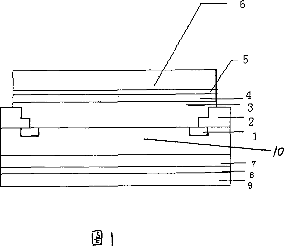
[0032] Accompanying drawing is a kind of specific embodiment of the present invention.

[0033] The barrier method of the power Schottky device of the present invention comprises the following steps: oxidation→first photolithography→boron diffusion→secondary photolithography→sputtering barrier metal→evaporating multi-layer metal on the front side→three photolithography→annealing→back reduction Thin → back evaporation → alloy → intermediate test and scribing and slicing

[0034] Power Schottky device potential barrier method of the present invention utilizes metal silicide MoSi 2 —Silicon contact replaces the traditional metal-semiconductor contact, which not only avoids surface defects and contamination, but also reduces the influence of surface states, thereby improving the forward characteristics, reverse withstand voltage and anti-burnout capabilities of the device. When choosing a barrier metal, the stability and reliability of the contact must be considered. Considering ...


PUM


Abstract

Characters of the method includes following steps: (1) oxidation; (2) first photo etching; (3) boron diffusion; (4) second photo etching; (5) sputtering barrier metal; (6) vaporizing multilayer of metal on face side; (7) third photo etching; (8) annealing; (9) thinning rear face; (10) vaporizing multilayer of metal on rear face; (11) alloying (12) testing and cutting to separate slices. Useful effects are: reducing influences from surface state, enhancing forward and backward characteristics as well as capability of inverted voltage resistant and anti burning, preventing oxidation of metal layer prolonging service life, avoiding interdiffusion between each metal and silicide, raising fatigue resistance, and reinforcing stability of parts.

Description

(1) Technical field [0001] The invention relates to a power schottky barrier diode chip manufacturing technology, in particular to a power schottky device potential barrier method. (2) Background technology [0002] Power Schottky devices are not only widely used in electronic information fields such as communications, computers, and automobiles, but also used in key national defense projects such as aviation and aerospace. Waste of electric energy, the electrical parameters of power Schottky devices mainly include: forward voltage drop, reverse voltage, reverse leakage, etc. Schottky devices produced by existing technology have the following disadvantages: [0003] 1. The traditional metal-semiconductor contact has a great influence on the surface state, and the forward characteristics, reverse characteristics, reverse withstand voltage and anti-burnout capabilities of the device are poor. [0004] 2. The annealing temperature is poorly controlled, which affects the perfor...

Claims


Application Information

Patent Timeline
Patent Type & Authority Applications(China)
IPC IPC(8): H01L21/329
Inventor 孙玉珍陈涛陈守迎董军孙卯秋李亚南王君平郭海燕郝思成张聪张建波时石田李庄
Owner JINAN JINGHENG ELECTRONICS
Why Eureka
Try Eureka