Device Handling Method

A processing method and device technology, applied in semiconductor devices, semiconductor/solid-state device manufacturing, electrical components, etc., can solve the problem of large forward voltage drop of devices, improve forward characteristics, improve roughness, and reduce positive voltage. The effect of the pressure drop

Active Publication Date: 2017-06-30
FOUNDER MICROELECTRONICS INT
View PDF5 Cites 0 Cited by
  • Summary
  • Abstract
  • Description
  • Claims
  • Application Information

AI Technical Summary

Problems solved by technology

[0004] The invention provides a device processing method, which is used to solve the problem that the current device processing method causes a large forward conduction voltage drop of the device

Method used


Image

  • Device Handling Method

Examples


Embodiment Construction

[0011] In order to make the purpose, technical solutions and advantages of the embodiments of the present invention more clear, the technical solutions in the embodiments of the present invention will be clearly and completely described below in conjunction with the drawings in the embodiments of the present invention.

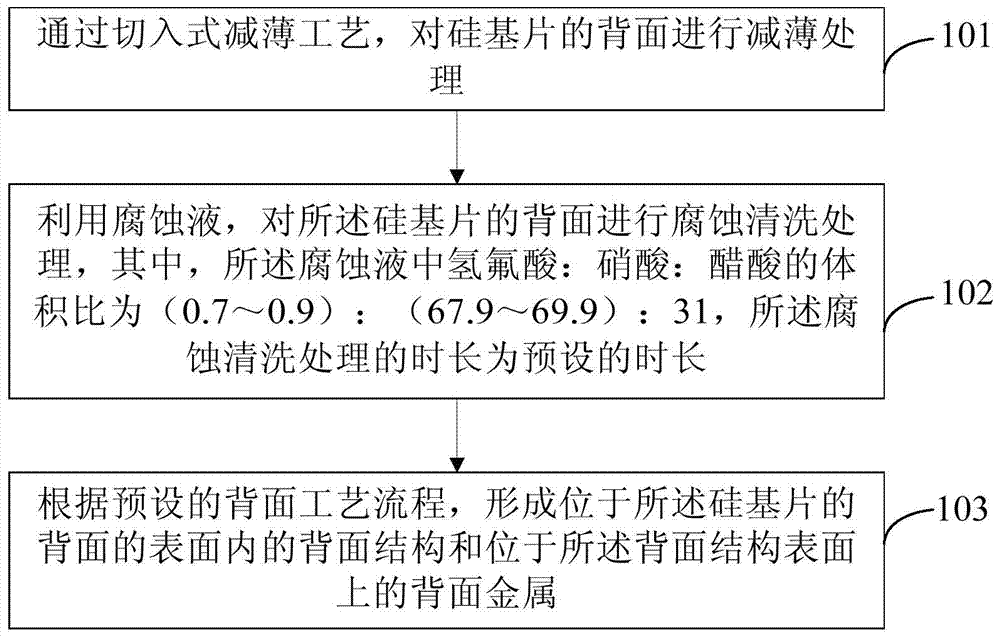
[0012] figure 1 A schematic flow chart of a device processing method provided in Embodiment 1 of the present invention, such as figure 1 As shown, the method includes:

[0013] 101. Thinning the back side of the silicon substrate through a cut-in thinning process.

[0014] Specifically, in practical applications, it is usually necessary to form the front structure of the device before performing the process flow of the back side of the device. Correspondingly, before step 101, the method may further include:

[0015] forming a front structure located in and on the front surface of the silicon substrate according to a preset front process flow;

[0016] A p...


PUM


Abstract

The invention provides a method for processing devices. The method includes thinning the backs of silicon substrates by the aid of cut-in thinning technologies, and carrying out corrosion cleaning processing on the backs of the silicon substrates for preset durations; forming back structures and back metal according to preset back technological processes. A volume ratio of hydrofluoric acid to nitric acid to acetic acid in corrosive liquid is (0.7-0.9):(67.9-69.9):31. The back structures are positioned in the surfaces of the backs of the silicon substrates, and the back metal is positioned on the surfaces of the back structures. The method for processing the devices has the advantages that the roughness of the surfaces of the substrates can be effectively improved, accordingly, forward voltage drop of the devices can be effectively reduced, and forward characteristics of the devices can be improved.

Description

technical field [0001] The invention relates to the field of semiconductor chip manufacturing technology, in particular to a device processing method. Background technique [0002] For a certain device, especially for a Vertical Double-diffused Metal Oxide Semiconductor (VDMOS) device, the magnitude of its forward conduction voltage drop is usually the same as that of the semiconductor on the backside of the silicon substrate and the metal on the backside. depends on the magnitude of the contact resistance. Furthermore, when the surface roughness of the semiconductor is too low, the adhesion between the semiconductor and the metal on the back will be reduced, resulting in a large contact resistance between the two, which in turn leads to a relatively large forward voltage drop of the device. [0003] In the existing device processing method, before the back structure of the device and the back metal on the surface of the back structure are formed in the back surface of the ...

Claims


Application Information

Patent Timeline
Patent Type & Authority Patents(China)
IPC IPC(8): H01L21/306H01L21/336
CPCH01L21/30608H01L29/66712
Inventor 赵圣哲
Owner FOUNDER MICROELECTRONICS INT
Why Eureka
Try Eureka