Schottky diode and manufacturing method thereof

A technology of Schottky diodes and manufacturing methods, applied in semiconductor/solid-state device manufacturing, electrical components, circuits, etc., can solve the problem of not being able to take full account of the problems, and achieve the effects of optimizing electrical parameter characteristics and low forward voltage drop.

Inactive Publication Date: 2012-05-16
上海芯石微电子有限公司
View PDF4 Cites 7 Cited by
  • Summary
  • Abstract
  • Description
  • Claims
  • Application Information

AI Technical Summary

Problems solved by technology

That is to say, it is not possible to give full consideration to both the on-state performance and the off-state performance.

Method used


Image

  • Schottky diode and manufacturing method thereof
  • Schottky diode and manufacturing method thereof
  • Schottky diode and manufacturing method thereof

Examples


Embodiment Construction

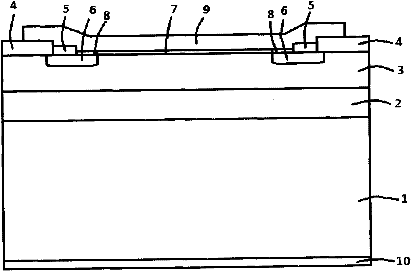
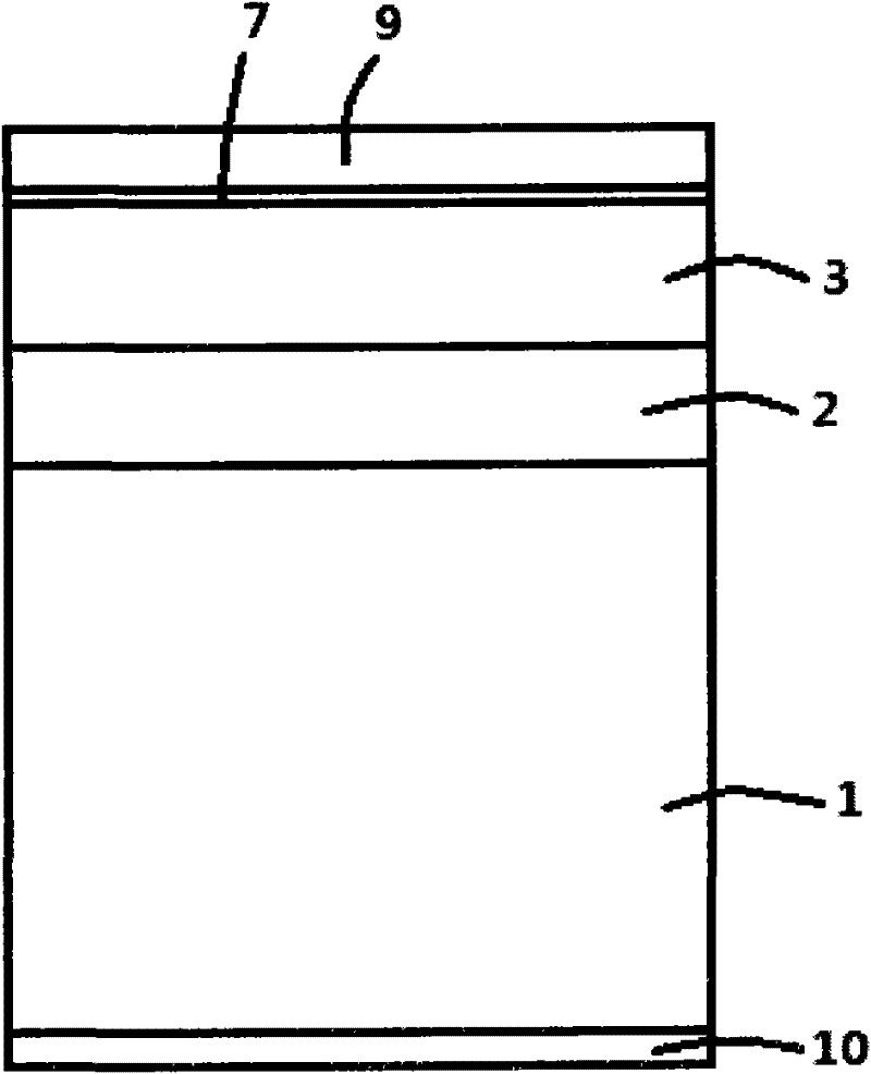
[0050] figure 1 Shows a schematic cross-sectional view of an embodiment of the present invention, combined below figure 1 The semiconductor device of the present invention will be described in detail.

[0051] A Schottky diode includes: a substrate layer 1, which is an N-conduction type silicon semiconductor material, and the cathode of the device is drawn out through a cathode metal layer 10 on the lower surface of the substrate layer; a buffer layer 2, located on the substrate layer 1, is an N-conduction type Silicon semiconductor material, the impurity concentration of this layer of semiconductor material gradually decreases as it moves away from the substrate layer; the drift layer 3, located on the buffer layer 2, is an N-conduction type silicon semiconductor material; the guard ring 6, located in the Schottky barrier layer 7 edge, the guard ring 6 is a P-conduction type silicon semiconductor material, the guard ring 6 is located in the drift layer 3, and the width of th...


PUM


Abstract

The invention discloses a novel schottky diode device. The device comprises a substrate layer, a gradual doping buffer layer, a drifting layer and a schottky barrier layer. The invention also provides a manufacturing method of a schottky diode. A semiconductor device provided by the invention has low forward voltage drop, and the electrical parameter characteristic of the device is further optimized.

Description

technical field [0001] The invention mainly relates to a semiconductor device, in particular to a Schottky diode and a manufacturing method thereof. Background technique [0002] Schottky diode is a device formed by contact between metal and semiconductor, which has low forward voltage drop and extremely high switching speed, but the unfavorable characteristics of large reverse leakage current and low reverse voltage affect the device within a certain range. applications within. [0003] For Schottky diodes, the forward voltage drop and reverse blocking voltage drop need to be selected in a compromise, because reducing the forward voltage drop will inevitably lead to a decrease in the reverse blocking voltage drop, and increasing the reverse blocking voltage drop. At the same time, it will inevitably cause an increase in the forward voltage drop. That is to say, it is impossible to fully consider both the on-state performance and the off-state performance. Contents of th...

Claims


Application Information

Patent Timeline
Patent Type & Authority Applications(China)
IPC IPC(8): H01L29/872H01L29/06H01L21/329
Inventor 杨忠武
Owner 上海芯石微电子有限公司
Why Eureka
Try Eureka