Semiconductor device

A semiconductor and depletion layer technology, applied in the structure and manufacturing process of junction barrier Schottky devices, can solve problems affecting device applications, low forward voltage drop switching speed, low reverse voltage, etc., and achieve electrical parameters Effects of characteristic optimization, reduction of reverse leakage current, and improvement of switching speed

Inactive Publication Date: 2010-05-12
ZHEJIANG UNIV
View PDF0 Cites 2 Cited by
  • Summary
  • Abstract
  • Description
  • Claims
  • Application Information

AI Technical Summary

Problems solved by technology

[0002] There are usually three kinds of rectifiers, (1) Schottky barrier diode, which is a metal and semiconductor contact device, has a low forward voltage drop and a very high switching speed, but has a large reverse leakage current and a reverse voltage Not high unfavorable characteristics affect the application of the device within a certain range
[0003] (2) P-i-N diodes provide lower leakage current and higher reverse voltage, but during the switching process, a certain amount of stored charge is stored on the PN junction, which affects the switching speed of the device
That is to say, it is not possible to give full consideration to both the on-state performance and the off-state performance.

Method used


Image

  • Semiconductor device
  • Semiconductor device
  • Semiconductor device

Examples


Embodiment 1

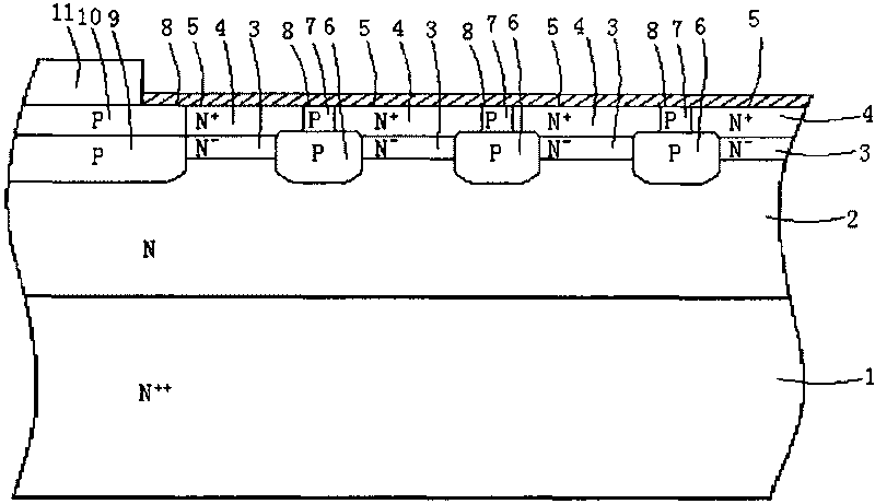
[0039] as attached figure 1 , attached figure 2 Shown is a schematic cross-sectional view and a top view of the first embodiment of the present invention.

[0040] The semiconductor device of the present invention includes: N-type substrate region 1, which is an N-type conductivity type semiconductor substrate material, and the cathode is drawn out through a metal on the lower surface of the substrate layer; N-type drift layer 2, which is an N-type conductivity type semiconductor material, is located On the N-type substrate region 1; the N-type depletion layer 3 is a semiconductor material of the N-type conductivity type, located on the N-type drift layer 2; the N-type heavily doped layer 4 is a semiconductor material of the N-type conductivity type, Located on the N-type depletion layer 3; the semiconductor material and metal on the top of the N-type heavily doped layer 4 form a Schottky barrier layer 5, and a layer of conductive metal is covered on the Schottky barrier lay...

Embodiment 2

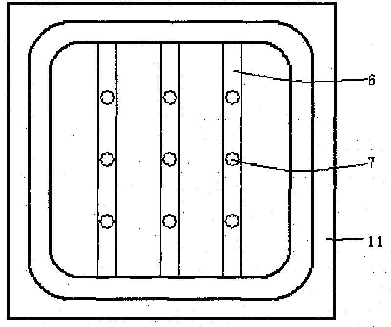
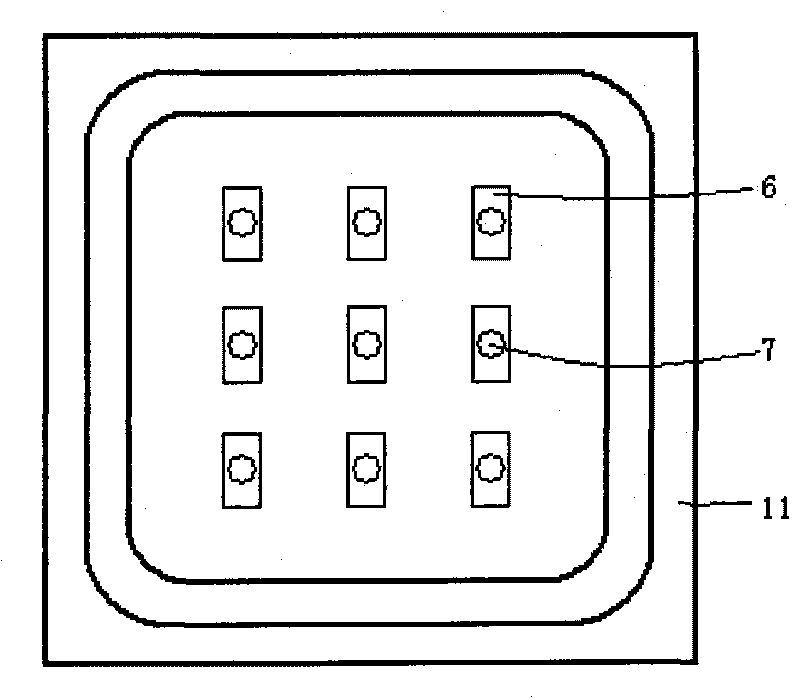
[0046] as attached image 3 As shown, nine strip-shaped reverse-bias leakage current suppression P-type regions 6 are separately formed in the N-type drift layer 2 and the N-type depletion layer 3, and the width of each reverse-bias leakage current suppression P-type region 6 is set The distance between two adjacent P-type regions 6 for suppressing reverse bias leakage current is 2-6um; nine small-area P-type regions 7 separated from each other are formed in the N-type heavily doped layer 4, each Two small-area P-type regions 7 are connected to corresponding reverse-bias leakage current suppressing P-type regions 6, the distance between two adjacent small-area P-type regions 7 is 2-20um, and the diameter of each small-area P-type region 7 circle is 1~5um; the phosphorus impurity concentration in the drift layer is 1×10 16 atom / cm 3 , the phosphorus impurity concentration in the depletion layer is chosen to be 1×10 15 atom / cm 3 , the concentration of phosphorus atoms doped ...

Embodiment 3

[0048] The structure and manufacturing process are as in Example 1, and the phosphorus impurity concentration in the drift layer is selected as 5×10 16 atom / cm 3 , the phosphorus impurity concentration in the depletion layer is chosen to be 5×10 15 atom / cm 3 , the concentration of doped phosphorus atoms in the substrate layer is selected as 1×10 20 atom / cm 3 , the phosphorus impurity concentration in the heavily doped layer is chosen to be 8×10 16 atom / cm 3 .


PUM


Abstract

The invention discloses a semiconductor device. The device comprises: a substrate layer, a drifting layer, a depletion layer, inhibited back biased leak current P type zones, a heavy doping layer, a schottky barrier layer and a small area P type zone, wherein a plurality of mutually separated inhibited back biased leak current P type zones are arranged in the drifting layer and the depletion layer and used for forming a large area of depletion zone in the semiconductor material of the depletion layer through expansion when the semiconductor device is applied with reverse bias voltage. The invention also provides a making method of the semiconductor device. The semiconductor device and the method can also reduce a certain amount of reverse leakage current while reducing a certain amount of forward voltage drop, simultaneously improve the switching speed of the device and further optimize the electric parameter properties of the device.

Description

technical field [0001] The present invention mainly relates to the structure and manufacturing process of a junction barrier Schottky device, in particular to the structure and manufacturing process of a novel junction barrier Schottky device with low forward voltage drop and low reverse leakage current at the same time . Background technique [0002] There are usually three kinds of rectifiers, (1) Schottky barrier diode, which is a metal and semiconductor contact device, has a low forward voltage drop and a very high switching speed, but has a large reverse leakage current and a reverse voltage The unfavorable characteristics that are not high affect the application of the device within a certain range. [0003] (2) P-i-N diodes provide lower leakage current and higher reverse voltage, but during the switching process, a certain amount of stored charge is stored on the PN junction, which affects the switching speed of the device. [0004] (3) Junction barrier controlled ...

Claims


Application Information

Patent Timeline
Patent Type & Authority Applications(China)
IPC IPC(8): H01L29/872H01L21/329
Inventor 朱江丁扣宝韩雁
Owner ZHEJIANG UNIV
Why Eureka
Try Eureka