Silicon carbide JBS device cellular structure with novel deep groove, and preparation method thereof

A deep trench and silicon carbide technology, which is applied in semiconductor/solid-state device manufacturing, semiconductor devices, electrical components, etc., to achieve the effects of increasing surge resistance, increasing P-type contact area, and improving device withstand voltage

Pending Publication Date: 2021-11-12
安徽长飞先进半导体有限公司
View PDF2 Cites 0 Cited by
  • Summary
  • Abstract
  • Description
  • Claims
  • Application Information

AI Technical Summary

Problems solved by technology

The SBD structure of a single-width trench requires a compromise between the trench depth and the forward conduction resistance of the device, and a compromise between the trench spacing and the withstand voltage and surface electric field strength of the Schottky region between the trenches. , which brings contradictions to the design of high withstand voltage SBD devices

Method used


Image

  • Silicon carbide JBS device cellular structure with novel deep groove, and preparation method thereof
  • Silicon carbide JBS device cellular structure with novel deep groove, and preparation method thereof
  • Silicon carbide JBS device cellular structure with novel deep groove, and preparation method thereof

Examples


Embodiment Construction

[0027] The specific implementation of the present invention will be described in further detail below by describing the embodiments with reference to the accompanying drawings, so as to help those skilled in the art have a more complete, accurate and in-depth understanding of the inventive concepts and technical solutions of the present invention.

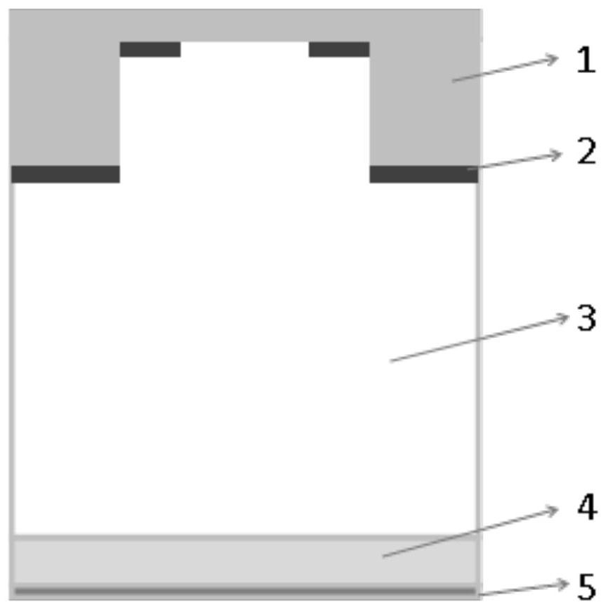
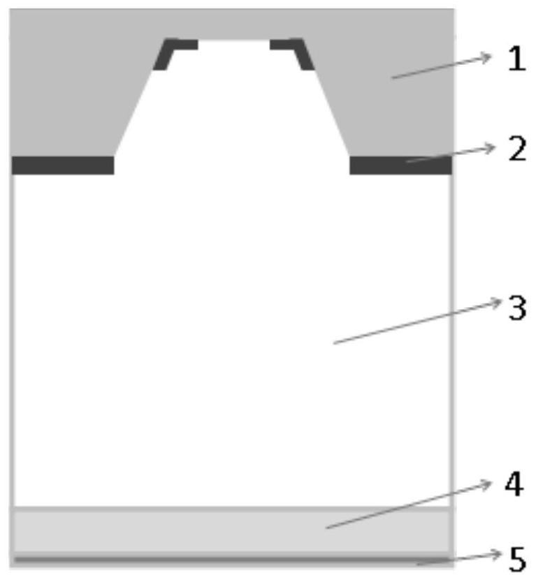
[0028] figure 1 The schematic diagram of the cell structure of a silicon carbide JBS device with rectangular deep trenches provided for the embodiment of the present invention, for the convenience of description, only shows the parts related to the embodiment of the present invention. The silicon carbide JBS device cell structure includes:

[0029] N+ type substrate, N-type epitaxial layer formed on the upper surface of N+ type substrate, rectangular trench formed above the N-type epitaxial layer, P+ type ion implantation at the bottom of the rectangular trench and at the top corner of the rectangular trench region, an N-type Scho...


PUM

PropertyMeasurementUnit
thicknessaaaaaaaaaa
depthaaaaaaaaaa
thicknessaaaaaaaaaa

Abstract

The invention discloses a silicon carbide JBS device cellular structure with a novel deep groove. The cellular structure comprises an N+ type substrate, an N- type epitaxial layer formed on the upper surface of the N+ type substrate, a groove formed above the N-type epitaxial layer, P+ type ion implantation regions located at the bottom of the groove and at the corner of the top of the groove, an N- type Schottky contact region positioned above the N-type epitaxial layer, and an N+ type ohmic contact region positioned below the substrate. The contradiction between forward conduction impedance of the device and Schottky region withstand voltage and surface electric field reliability caused by a groove structure during device design can be avoided, a transverse Schottky contact channel is added during forward conduction, and forward conduction resistance is greatly reduced; under the surge condition, the P-type contact area is increased, and the surge resistance is improved; and through multi-layer P-type injection cooperative protection, the withstand voltage of the Schottky region and the reliability of the surface electric field can be effectively improved.

Description

technical field [0001] The invention belongs to the technical field of semiconductors, and more specifically, the invention relates to a silicon carbide JBS device cell structure with novel deep grooves and a preparation method thereof. Background technique [0002] Wide bandgap semiconductor materials are third-generation semiconductor materials represented by materials such as silicon carbide and gallium nitride. SiC materials have developed rapidly in recent years. The SiC material has a large band gap, which can reach more than 3eV, and has excellent radiation resistance. The critical breakdown electric field can reach more than 2MV / cm. SiC material has high thermal conductivity (about 4.9W / cm.K), and the device is resistant to high temperature, which is more suitable for high-current devices than Si. Therefore, since the 1990s, power devices such as SiC MOSFETs and SBDs have been widely used in switching regulated power supplies, high-frequency heating, automotive ele...

Claims


Application Information

Patent Timeline
Patent Type & Authority Applications(China)
IPC IPC(8): H01L29/06H01L29/872H01L21/329
CPCH01L29/872H01L29/6606H01L29/0696H01L29/0684H01L29/0615
Inventor 史文华钮应喜乔庆楠罗峥嵘史田超彭强袁松张晓洪单卫平王敬
Owner 安徽长飞先进半导体有限公司
Why Eureka
Try Eureka