A kind of ohmic contact forming method of sic wafer

A technology of ohmic contact and wafer, which is applied in the direction of electrical components, semiconductor/solid-state device manufacturing, circuits, etc., can solve the problems of contact metal oxidation, device performance impact, and process complexity in SiC devices, and achieve positive characteristic improvement and removal Effect of carbon residue and simplified treatment process

Active Publication Date: 2017-12-08
ZHUZHOU CRRC TIMES SEMICON CO LTD
View PDF5 Cites 0 Cited by
  • Summary
  • Abstract
  • Description
  • Claims
  • Application Information

AI Technical Summary

Problems solved by technology

[0007] Although the oxygen plasma carbon removal method can effectively remove the thin layer of carbon on the surface of SiC devices, this method is not only complicated in process, but also causes the oxidation of the contact metal in the SiC device, which requires additional process treatment after the carbon removal process to be oxidized contact metal, leading to further complication of the whole SiC wafer ohmic contact process
In addition, if the thin layer of carbon and the oxidized ohmic contact metal are not removed completely, it will seriously affect the device performance

Method used


Image

  • A kind of ohmic contact forming method of sic wafer
  • A kind of ohmic contact forming method of sic wafer
  • A kind of ohmic contact forming method of sic wafer

Examples


Embodiment 1

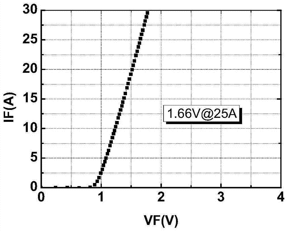
[0041] Fabrication of SiC wafers forming ohmic contacts

[0042] 1) Ohmic contact metal deposition: use magnetron sputtering method to deposit ohmic contact metal on the surface of SiC wafer (4 inches × 400μm), the target material is Ni, the sputtering pressure is set to 0.5 ~ 1Pa, and the magnetron sputtering ends After that, a SiC wafer with a Ni layer of 200-220 nm deposited on the surface is obtained.

[0043] 2) Metal alloying annealing: place the SiC wafer with a Ni layer deposited on the surface in a high-temperature rapid annealing furnace; pass in argon gas, and when the oxygen content monitoring system shows that the oxygen content inside the equipment cavity is less than 20-30ppm, start Heating, the temperature is raised to 950-975°C at a heating rate of 20°C / s, and maintained at this temperature for 5 minutes; the temperature is naturally lowered, and when the temperature drops to 200-300°C, CO is introduced into the annealing furnace 2 gas to fully expose the SiC...

Embodiment 2

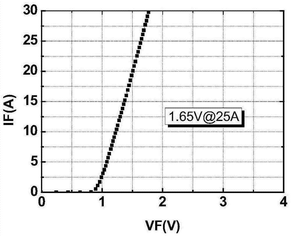
[0045] Fabrication of SiC wafers forming ohmic contacts

[0046] 1) Ohmic contact metal deposition: use magnetron sputtering method to deposit ohmic contact metal on the surface of SiC wafer (4 inches × 400μm), the target material is Ni, the sputtering pressure is set to 0.5 ~ 1Pa, and the magnetron sputtering ends After that, a SiC wafer with a Ni layer of 230-250 nm deposited on the surface is obtained.

[0047] 2) Metal alloying annealing: place the SiC wafer with a Ni layer deposited on the surface in a high-temperature rapid annealing furnace; pass in argon gas, and when the oxygen content monitoring system shows that the oxygen content inside the equipment cavity is less than 20-30ppm, start Heating, raise the temperature to 970-990°C at a heating rate of 25°C / s, and maintain at this temperature for 3 minutes; naturally cool down, when the temperature drops to 200-300°C, pass CO into the annealing furnace 2 gas to fully expose the SiC wafer to CO 2 In the atmosphere, m...

Embodiment 3

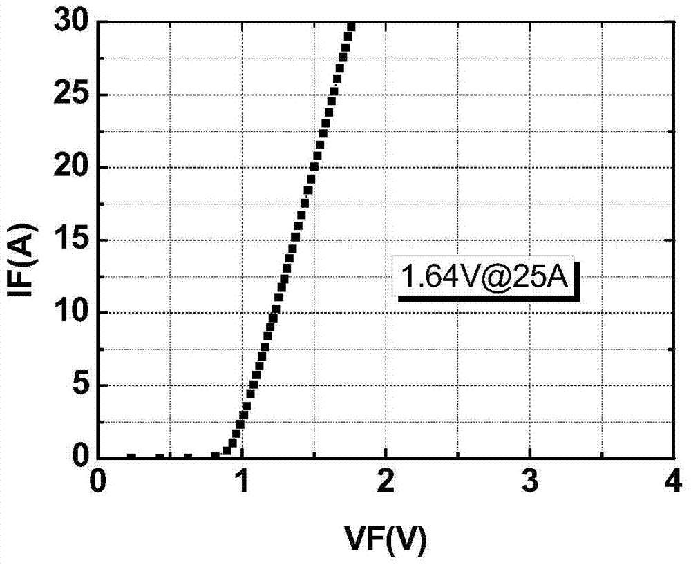
[0049] Fabrication of SiC wafers forming ohmic contacts

[0050] 1) Ohmic contact metal deposition: use magnetron sputtering method to deposit ohmic contact metal on the surface of SiC wafer (4 inches × 400μm), the target material is Ni, the sputtering pressure is set to 0.5 ~ 1Pa, and the magnetron sputtering ends After that, a SiC wafer with a Ni layer of 280-300 nm deposited on the surface is obtained.

[0051] 2) Metal alloying annealing: place the SiC wafer with a Ni layer deposited on the surface in a high-temperature rapid annealing furnace; pass in argon gas, and when the oxygen content monitoring system shows that the oxygen content inside the equipment cavity is less than 20-30ppm, start Heating, raise the temperature to 1025-1050°C at a heating rate of 30°C / s, and maintain at this temperature for 2 minutes; naturally cool down, when the temperature drops to 200-300°C, pass CO into the annealing furnace 2 gas to fully expose the SiC wafer to CO 2 In the atmosphere,...


PUM

PropertyMeasurementUnit
thicknessaaaaaaaaaa

Abstract

The invention belongs to the SiC field, and particularly relates to the SiC wafer ohmic contact formation method. The SiC wafer ohmic contact formation method comprises steps of a) deposing a metal level on a surface of an SiC wafer to obtain an SiC wafer having the deposition metal layer on the surface, and b) performing annealing on the SiC wafer having the deposition metal layer on the surface to obtain an SiC wafer forming the ohmic contact; the annealing process comprises a plurality of temperature rising stages, a plurality of temperature holding stages and a plurality of cooling stages; and at least one stage in the annealing process is proceeded in the CO2 atmosphere. In the SiC wafer ohmic contact formation method disclosed by the invention, the CO2 gas enters in the process of annealing of the SiC wafer having the deposition metal layer, the CO2 gas reacts with the simple substance carbon generated during the annealing process and the effective removing of the simple substance carbon in the annealing process is realized. The invention greatly simplifies the processing process of the SiC wafer ohmic contact technology without the extra carbon removing technology.

Description

technical field [0001] The invention belongs to the field of SiC, and in particular relates to a method for forming an ohmic contact of a SiC wafer. Background technique [0002] As a third-generation semiconductor material, SiC material has many unique advantages, such as: high breakdown electric field, low on-resistance, high thermal conductivity and high saturation electron mobility. Therefore, SiC devices have higher withstand voltage capacity, lower on-resistance, and better thermal conductivity. Since SiC devices have the above-mentioned many advantages, people pay more and more attention to them, and become a semiconductor device with very broad application prospects. [0003] The preparation of SiC devices is very complicated, including many processes such as SiC film growth, ion doping, plasma etching, and ohmic contact formation. Among them, the formation of ohmic contacts is one of the most important processes for preparing SiC devices, and the quality of ohmic ...

Claims


Application Information

Patent Timeline
Patent Type & Authority Patents(China)
IPC IPC(8): H01L21/283
CPCH01L21/283
Inventor 史晶晶李诚瞻杨程刘国友刘可安
Owner ZHUZHOU CRRC TIMES SEMICON CO LTD
Why Eureka
Try Eureka