Method for manufacturing window plug holes at two sides during PCB (Printed Circuit Board) resistance welding

A technology of PCB board and manufacturing method, which is applied in the direction of electrical connection formation of printed components, can solve the problems of punching through plug holes, vomiting oil, etc., and achieve the effect of improving the punching through of plug holes

Active Publication Date: 2012-03-14
DONGGUAN SHENGYI ELECTRONICS
View PDF5 Cites 28 Cited by
  • Summary
  • Abstract
  • Description
  • Claims
  • Application Information

AI Technical Summary

Problems solved by technology

When this solder mask process is used for production, it is easy to have quality defects such as punching through the plug hole or vomiting oil, which needs to be improved

Method used


Image

  • Method for manufacturing window plug holes at two sides during PCB (Printed Circuit Board) resistance welding
  • Method for manufacturing window plug holes at two sides during PCB (Printed Circuit Board) resistance welding
  • Method for manufacturing window plug holes at two sides during PCB (Printed Circuit Board) resistance welding

Examples


Embodiment Construction

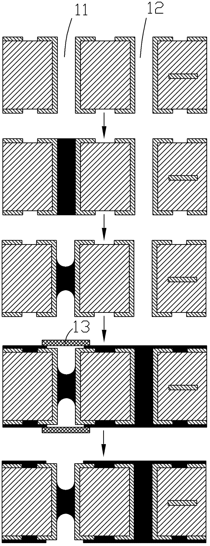
[0017] Such as figure 1 and figure 2 As shown, the manufacturing method of opening the window plug hole on both sides of the PCB board solder resistance of the present invention comprises the following steps:

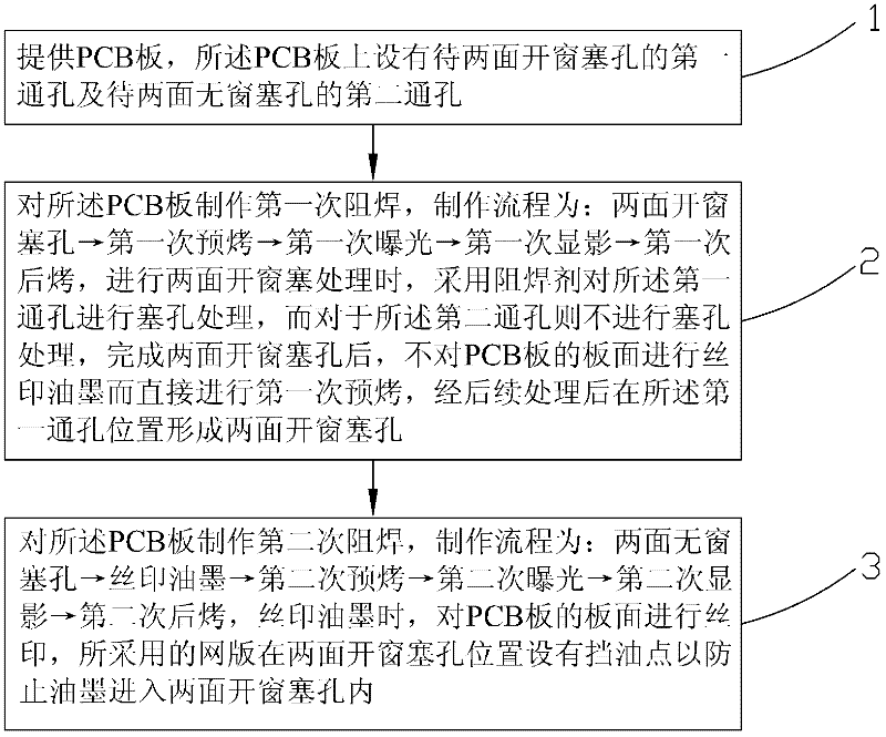
[0018] Step 1: Provide a PCB board, and the PCB board is provided with a first through hole 11 to be opened with windows on both sides and a second through hole 12 to have no window plug holes on both sides;

[0019] Step 2: Make the first solder resist on the PCB board. The production process is: open the window plug hole on both sides → the first pre-baking → the first exposure → the first development → the first post-baking, and perform double-sided opening During the window plug treatment, the first through hole 11 is plugged with solder resist, but the second through hole 12 is not plugged. After the window plug holes are opened on both sides, the PCB board The first pre-baking is directly carried out with screen printing ink on the surface, and after subsequent...


PUM


Abstract

The invention relates to a method for manufacturing window plug holes at two sides during PCB (Printed Circuit Board) resistance welding, comprising the following steps of: firstly, providing a PCB board, wherein the PCB board is provided with a first through hole to be provided with the window plug holes at the two sides and a second through hole not to be provided with the window plug holes at the two sides; secondly, carrying out primary resistance welding on the PCB board, wherein a manufacturing process comprises the following steps of: manufacturing the window plug holes at the two sides, carrying out primary prebaking, carrying out primary exposing, carrying out primary developing and carrying out primary after baking, and directly carrying out the primary prebaking without carrying out silk screen printing on the panel of the PCB board after the window plug holes are manufactured at the two sides; and thirdly, carrying out secondary resistance welding on the PCB board, whereinthe manufacturing process comprises the following steps of: manufacturing no window plug hole at the two sides, carrying out the silk screen printing, carrying out secondary prebaking, carrying out secondary exposing, carrying out secondary developing and carrying out secondary after baking. In the method for manufacturing the window plug holes at the two sides during PCB resistance welding, an independent plug hole process is adopted for manufacturing the window plug holes at the two sides, and the defects that the plug hole is punched through and oil is spewed can be effectively overcome.

Description

technical field [0001] The invention relates to the field of printed circuit board (Printed Circuit Board, PCB) manufacture, in particular to a method for manufacturing a PCB board with windows and plug holes on both sides of the solder resist. Background technique [0002] At present, when the PCB board with windows on both sides is subjected to solder resist processing, the following solder resist process is usually adopted: plugging → silk screen printing ink → pre-baking → exposure → development → board inspection → post-baking. When this solder mask process is used for production, it is easy to have quality defects such as punching through the plug hole or vomiting oil, which needs to be improved. Contents of the invention [0003] Therefore, the object of the present invention is to provide a method for manufacturing plug holes with windows on both sides of the PCB board, which adopts a separate plug hole process for the plug holes with windows on both sides, and eff...

Claims


Application Information

Patent Timeline
Patent Type & Authority Applications(China)
IPC IPC(8): H05K3/40
Inventor 邢玉伟易雁曾红曾志军
Owner DONGGUAN SHENGYI ELECTRONICS
Why Eureka
Try Eureka