

Sheet and light-emitting device
A technology of thin film and luminous body, applied in lighting devices, electroluminescent light sources, optics, etc., can solve problems such as increased product cost
Active Publication Date: 2012-03-28
PANASONIC CORP
View PDF7 Cites 0 Cited by
- Summary
- Abstract
- Description
- Claims
- Application Information
AI Technical Summary
Problems solved by technology
This leads to an increase in product cost
[0024] On the other hand, the light-emitting device disclosed in Patent Document 2 aims to prevent light from being reflected on the refracting surface, and this structure improves the light extraction efficiency by about 10% or 20%, which is very small.
Method used
View moreImage
Smart ImageViewing Examples

Examples
no. 1 approach
no. 2 approach
no. 3 approach
Login to View More PUM
| Property | Measurement | Unit |
|---|---|---|
| wavelength | aaaaa | aaaaa |
| transmittivity | aaaaa | aaaaa |
| refractive index | aaaaa | aaaaa |
Abstract
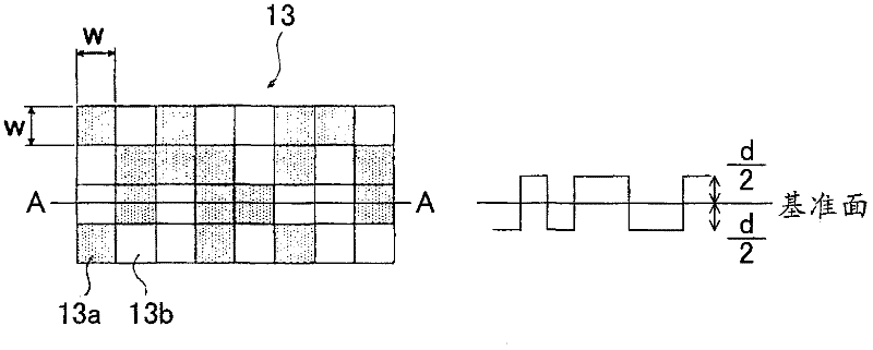
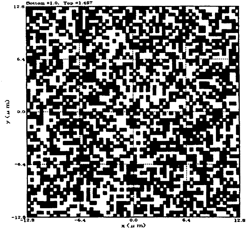
A sheet and a light emitting device are provided which also emit light having an incident angle larger than or equal to a critical angle to significantly increase light extraction efficiency, prevent ambient light reflection, and suppress the occurrence of a distribution of light intensity varying depending on the direction and an imbalance in color. The light emitting device has a surface structure (13) in a surface adjacent to a light emitting element of a transparent substrate (5). The surface of the transparent substrate (5) is virtually divided into minute regions without a gap, the diameter of a largest circle inscribed in the minute region being 0. 2 [mu]m or more and 1.5 [mu]m or less. Each minute region has a convex or concave shape in the surface of the transparent substrate 5. The proportions of the convex shapes and the concave shapes are P and 1-P, respectively, where P is within the range of 0.4 to 0.98.
Description
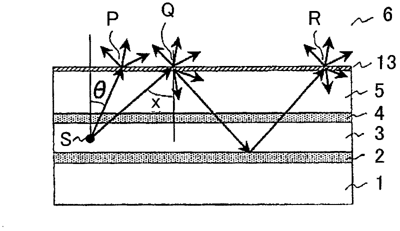
[0001] This application is a divisional application of the international application with the application number 200880001505.2 (international application number PCT / JP2008 / 003299) filed by the applicant on November 12, 2008, and the invention name is thin film and light emitting device. The application has entered the national phase The date is June 26, 2009. technical field [0002] The present invention relates to a transparent film with one surface adjacent to a luminous body and a light-emitting device using the transparent film. Background technique [0003] Conventional techniques include techniques disclosed in Patent Documents 1 and 2, for example. [0004] Figure 14 Shows the cross-sectional structure and light propagation of a light-emitting device using a common organic EL (electroluminescence) element. The electrode 102 , the luminescent layer 103 and the transparent electrode 104 are laminated on the substrate 101 in this order, and the transparent electrode ...
Claims
Login to View More Application Information
Patent Timeline
 Patent Type & AuthorityApplications(China)
IPC IPC(8): G02B5/02G02B5/18B32B3/30H01L51/52H05B33/22
CPCH01L51/5268G02B5/18H05B33/22G02B5/0221H10K50/854
Inventor西胁青儿
OwnerPANASONIC CORP