Electro-optic device, substrate for electro-optic device and method for manufacturing the same, photomask, and electronic device

An electro-optical device and mask technology, which can be used in microlithography exposure equipment, optomechanical equipment, photolithographic process exposure devices, etc., can solve the problems of insufficient light scattering and the like

Inactive Publication Date: 2005-05-18
SEIKO EPSON CORP
View PDF1 Cites 0 Cited by
  • Summary
  • Abstract
  • Description
  • Claims
  • Application Information

AI Technical Summary

Problems solved by technology

However, when this method is used, since a flat surface reflecting the plate surface of the substrate exposed between the resin sheets and the flat surface of the top of each resin sheet appears on the surface of the reflective layer, light scattering cannot be sufficiently obtained. The problem of the effect (hereinafter referred to as "light scattering effect")

Method used


Image

  • Electro-optic device, substrate for electro-optic device and method for manufacturing the same, photomask, and electronic device
  • Electro-optic device, substrate for electro-optic device and method for manufacturing the same, photomask, and electronic device
  • Electro-optic device, substrate for electro-optic device and method for manufacturing the same, photomask, and electronic device

Examples


Embodiment Construction

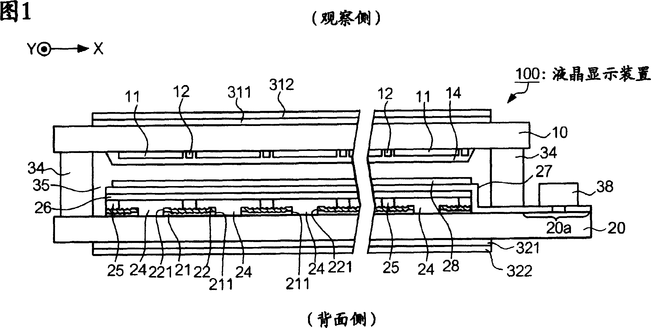
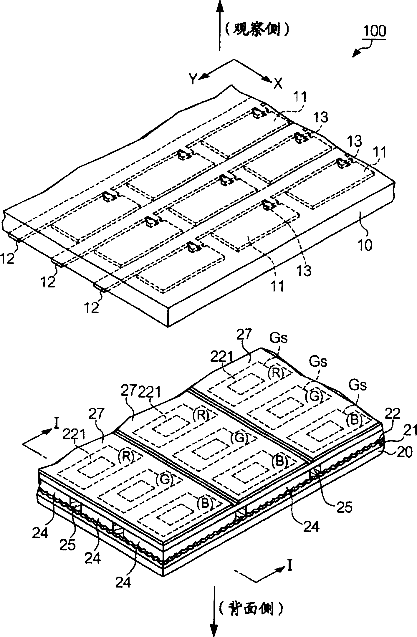
[0052] Embodiments of the present invention will be described below with reference to the drawings. The following exemplifies the application of the present invention to a liquid crystal display device using a liquid crystal as an electro-optical device, but it is not intended to limit the applicable range of the present invention. In addition, in each of the drawings shown below, the dimensions and ratios of the respective constituent elements are different from actual ones for convenience of description.

[0053]

[0054]

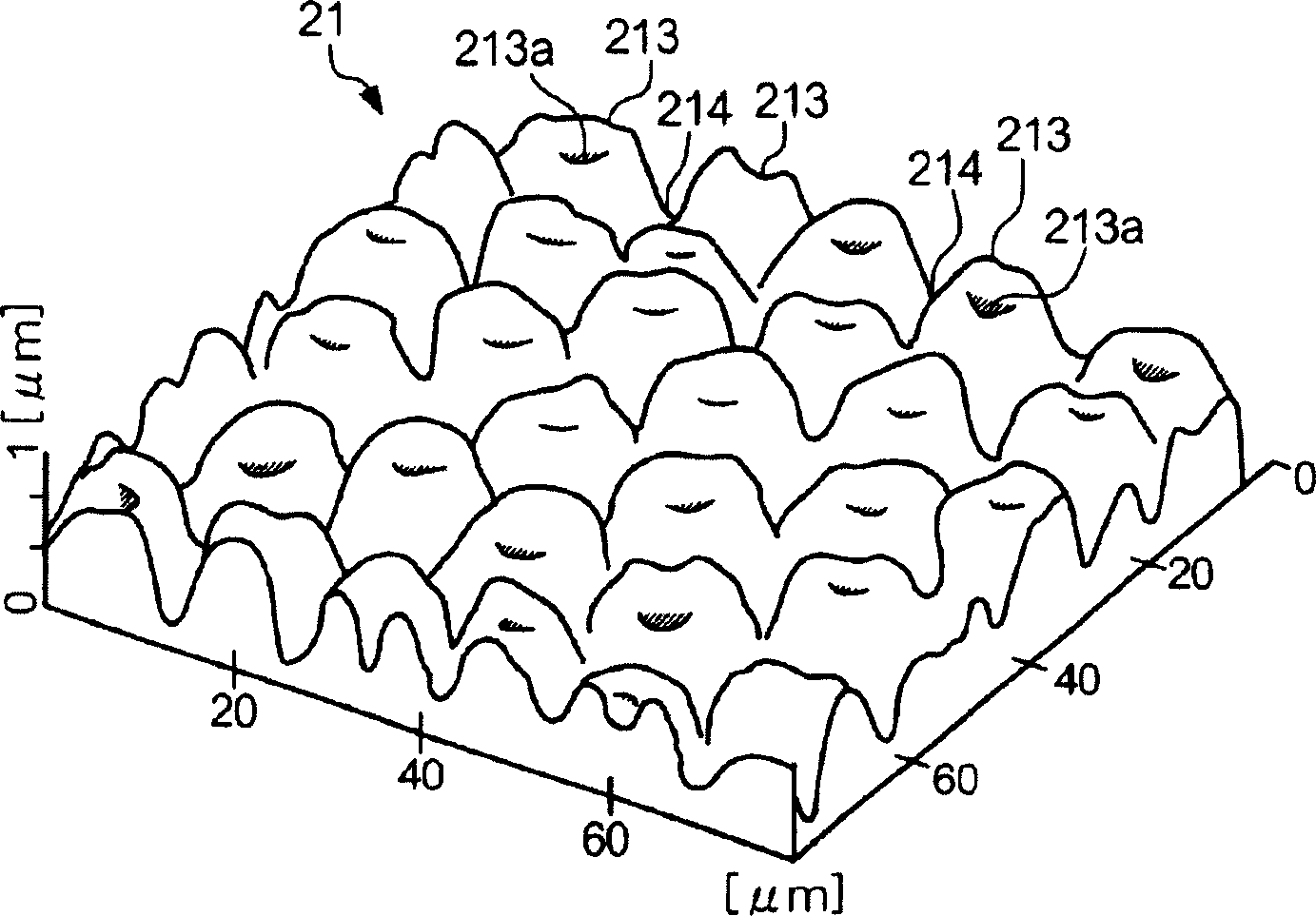
[0055] FIG. 1 is a cross-sectional view showing the configuration of a liquid crystal display device according to this embodiment, figure 2 It is an enlarged perspective view showing a part of this liquid crystal display device. From figure 2 The cross-sectional view of the I-I line observation is equivalent to that in Figure 1. As shown in these figures, the liquid crystal display device 100 has a first substrate 10 and a second substrate 20 tha...


PUM

PropertyMeasurementUnit
widthaaaaaaaaaa
diameteraaaaaaaaaa
transmittivityaaaaaaaaaa

Abstract

The present invention can obtain a reflective layer with good light scattering effect by means of a simple manufacturing process. The exposure mask 7 a of the present invention is used in an exposure process for making the processed region 511 of the film body 51 a rough surface. This exposure mask 7 a has a first region 71 and a second region 72 . Among them, the first region 71 is used as a light-transmitting portion 81 that transmits light directed toward the periphery of the region to be processed 511 . On the other hand, while the second region 72 includes a plurality of dot regions 721 in which the light shielding portions 84 for shielding the light incident on the region 511 to be processed are respectively provided, the region other than the dot region 721 is provided so as to be lower than the light transmitting portion 81. The light transmittance of the semi-transmissive portion 86 transmits the light incident on the region 511 to be processed.

Description

technical field [0001] The present invention relates to a technique for scattering reflected light by roughening the surface of a reflective layer. Background technique [0002] In a so-called reflective liquid crystal display device, a reflective layer having light reflectivity is formed on a surface of a substrate holding liquid crystal. Then, external light such as sunlight and indoor lighting incident from the observation side is reflected by the surface of the reflective layer, and the reflected light is used for image display. In this configuration, when the surface of the reflective layer is completely flat, the light incident on the liquid crystal display device is reflected by the surface of the reflective layer and can be recognized by the observer. In this case, there is a problem that it is difficult to observe the display because images of persons and objects facing the display surface of the liquid crystal display device can be viewed in addition to the origin...

Claims


Application Information

Patent Timeline
Patent Type & Authority Applications(China)
IPC IPC(8): G02F1/13G02F1/1335G03F1/00G03F7/00
CPCG02F1/133555G03F7/0005G03F1/50G02F1/1335G02F1/13
Inventor 中野智之金子英树大竹俊裕泷泽圭二
Owner SEIKO EPSON CORP
Why Eureka
Try Eureka