Nano hot stamping device

A hot embossing and nanotechnology, applied in optics, opto-mechanical equipment, instruments, etc., can solve the problems of unevenness, unbalanced force, uneven surface, etc., and achieve the effect of stable product quality, low cost and convenient operation.

Inactive Publication Date: 2012-05-02
SUZHOU GUANGDUO MICRO NANO DEVICE
View PDF5 Cites 10 Cited by
  • Summary
  • Abstract
  • Description
  • Claims
  • Application Information

AI Technical Summary

Problems solved by technology

[0005] The purpose of the present invention is to provide a nano-thermal embossing device, which overcomes the above-mentioned deficiencies in the prior art, and solves the unbalanced, uneven, and uneven surface conditions that tend to occur in mechanical thermal embossing or semi-mechanical thermal embossing. Vertically causes the problem of product defects and makes the equipment simple

Method used


Image

  • Nano hot stamping device
  • Nano hot stamping device

Examples


Embodiment Construction

[0016] The present invention will be described in further detail below in conjunction with the accompanying drawings and specific embodiments.

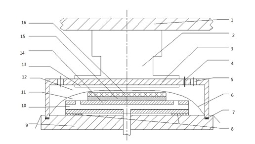
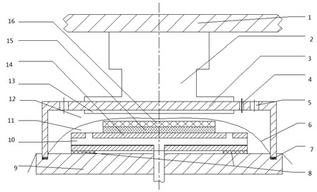
[0017] As shown in the drawings, the nano-thermal embossing device of the present invention includes a mold 16, a blank 15, a heating plate 14, a base 9, and a cavity 3. The heating plate 14 is placed on the base 9, and the blank 15 is placed on the heating plate 14. The mold 16 is placed on the blank 15, the cavity 3 and the base 9 are movably sealed to form an airtight space, the mold 16, the blank 15 and the heating plate 14 are enclosed in the airtight space, and a film 6 is also arranged in the cavity 3, and the film 6 It is fixed at the sealed contact surface between the cavity body 3 and the base 9, and the closed space formed by the cavity body and the base is divided into a pressure cavity 12 and a vacuum cavity 11, the pressure cavity 12 communicates with the air inlet 5, and the vacuum cavity 11 communicates with the exhaust...


PUM


Abstract

The invention discloses a nano hot stamping device which comprises a mould (16), a blank (15), a heating plate (14), a base (9) and a cavity (3), wherein the cavity (3) and the base (9) are movably sealed to form an enclosed space; the mould (16), the blank (15) and the heating plate (14) are closed in the enclosed space; a film (6) is also arranged in the cavity (3); the film (6) is fixed on a sealing contact surface of the cavity (3) and the base (9), and the enclosed space formed by the cavity and the base is divided into a pressure cavity (12) and a vacuum cavity (11); the pressure cavity (12) is communicated with an air inlet channel (5); and the vacuum cavity (11) is communicated with an air exhaust channel (10). According to the invention, a nano stamping die core is balanced and uniform and is pressed into a stamping base plate in a mode of being vertical to the surface; and the product is stable in quality, simple in structure and convenient to operate.

Description

technical field [0001] The invention relates to the technical field of nano processing, in particular to a thermal embossing device which utilizes air pressure to realize transfer of nano patterns. Background technique [0002] Nanoimprint technology is a cheap and high-resolution nano-pattern transfer technology. Graphic transfer is achieved by pressing a stamp with a nano-concave-convex structure (nanoimprint core) onto a thin polymer substrate (nanoimprint substrate); the device is heated or irradiated with ultraviolet light, and when the stamp is removed, the lining An imprint of the original concave-convex nanostructure pattern is left on the substrate. Among them, the balance, uniformity, and perpendicularity of the indentation of the nanoimprint mold core are the keys to the nanoimprint process. Any slight imbalance, non-uniformity, and non-perpendicularity to the surface of the indentation will distort the pattern transfer. [0003] Chinese Invention Patent Authori...

Claims


Application Information

Patent Timeline
Patent Type & Authority Applications(China)
IPC IPC(8): G03F7/00
Inventor 史晓华冀然陈沁薛愉峰
Owner SUZHOU GUANGDUO MICRO NANO DEVICE
Why Eureka
Try Eureka