Global shutter pixel unit of complementary metal oxide semiconductor (CMOS) image sensor

An image sensor and global exposure technology, which is applied in image communication, electrical components, televisions, etc., can solve the problem of large pixel noise in global exposure, and achieve the effects of good preservation, total noise reduction, and small leakage

Active Publication Date: 2013-09-04
INST OF SEMICONDUCTORS - CHINESE ACAD OF SCI
View PDF4 Cites 2 Cited by
  • Summary
  • Abstract
  • Description
  • Claims
  • Application Information

AI Technical Summary

Problems solved by technology

[0008] In view of this, the main purpose of the present invention is to provide a CMOS image sensor global exposure with low noise, large dynamic range, small pixel area, and high light-shielding efficiency in order to solve the problem of large pixel noise in the existing global exposure in the CMOS image sensor. pixel unit

Method used


Image

  • Global shutter pixel unit of complementary metal oxide semiconductor (CMOS) image sensor
  • Global shutter pixel unit of complementary metal oxide semiconductor (CMOS) image sensor
  • Global shutter pixel unit of complementary metal oxide semiconductor (CMOS) image sensor

Examples


Embodiment 1

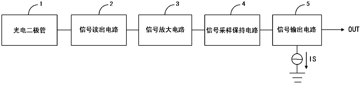
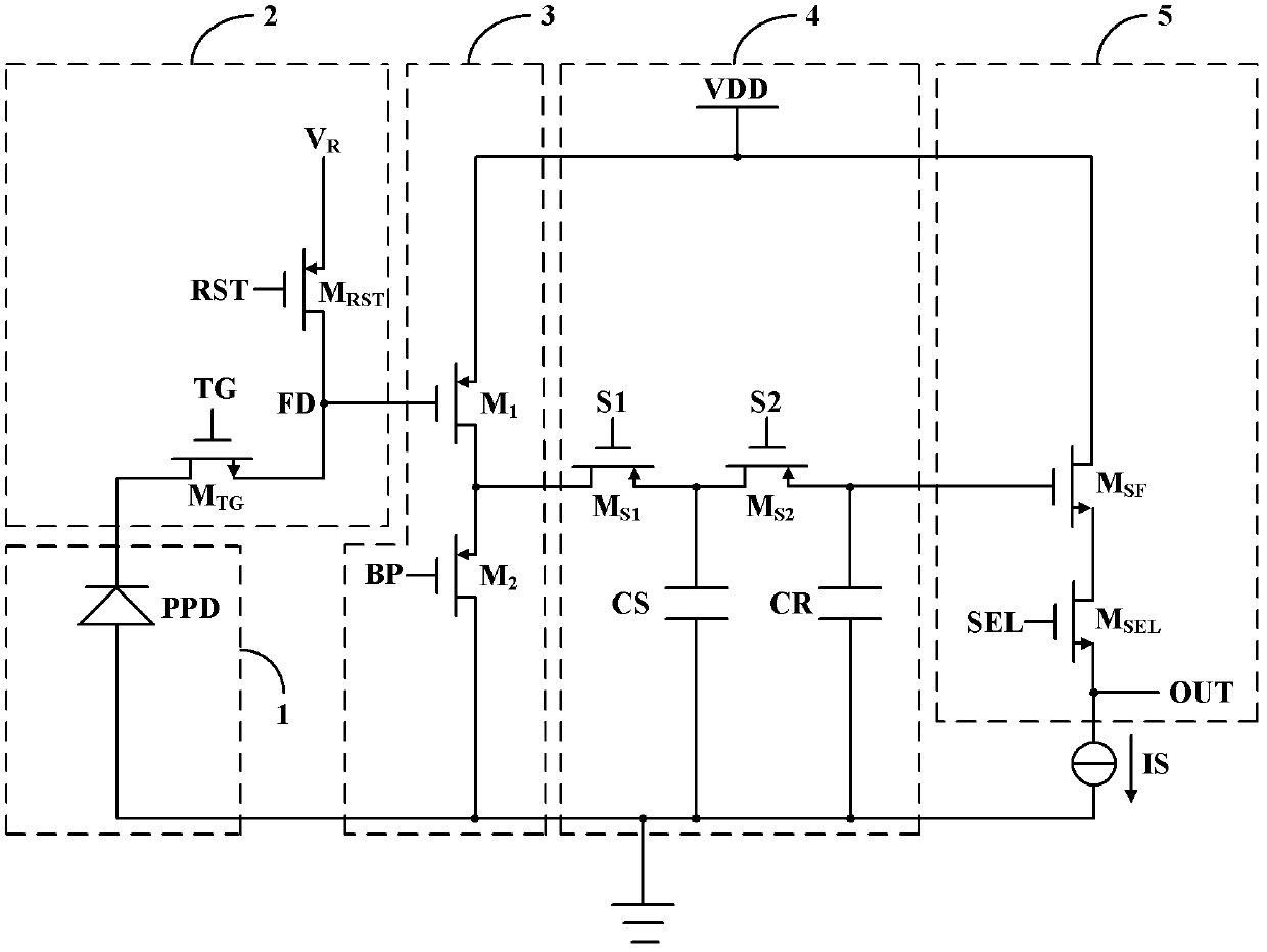
[0045] like figure 2 as shown, figure 2 It is a circuit diagram of the global exposure pixel unit of the CMOS image sensor according to the first embodiment of the present invention. Photodiode 1 consists of a buried layer photodiode PPD. The signal readout circuit 2 consists of an N-type MOS transmission tube M TG And a P-type MOS reset transistor M RST composition. The signal amplifying circuit 3 consists of two P-type MOS transistors M 1 , M 2 Composition, these two P-type MOS transistors form an operational amplifier. The signal sampling and holding circuit 4 is composed of a first P-type MOS switch tube M S1 , the second P-type MOS switch tube M S2 , composed of the first sampling and holding capacitor CS and the second sampling and holding capacitor CR. The signal output circuit 5 consists of an N-type MOS source follower M SF And an N-type MOS row gate tube M SEL composition. The pixel external current source IS constitutes a load of the signal output circ...

Embodiment 2

[0075] Figure 4 It is a circuit diagram of the global exposure pixel unit of the CMOS image sensor according to the second embodiment of the present invention. The photodiode 1 consists of an ordinary photodiode PD. The signal readout circuit 2 consists of an N-type MOS transmission tube M TG And an N-type MOS reset transistor M RST composition. The signal amplifying circuit 3 consists of two P-type MOS transistors M 1 , M 2 and a resistor R, these two P-type MOS transistors and the resistor R form an operational amplifier. The signal sampling and holding circuit 4 is composed of a first N-type MOS switch tube M S1 , the second N-type MOS switch M S2 , composed of the first sampling and holding capacitor CS and the second sampling and holding capacitor CR. The signal output circuit 5 consists of an N-type MOS source follower M SF And an N-type MOS row gate tube M SEL composition. The pixel external current source IS constitutes a load of the signal output circuit 5...


PUM


Abstract

The invention discloses a global shutter pixel unit of a complementary metal oxide semiconductor (CMOS) image sensor. The global shutter pixel unit comprises a photoelectric diode, a signal readout circuit, a signal amplifying circuit, a signal sampling and retaining circuit and a signal output circuit which are connected with one another, wherein the photoelectric diode is used for acquiring original information of an incident light ray and converting an acquired target image light signal into an electric signal; the signal readout circuit is used for reading the electric signal subjected to photoelectric conversion in the photoelectric diode out, and storing the electric signal in a node FD; the signal in the node FD is amplified by the signal amplifying circuit; the signal amplifying circuit comprises an operational amplifier which is used for amplifying the signal stored in the node FD; the amplified signal is output to the signal sampling and retaining circuit; the signal sampling and retaining circuit is used for sampling and retaining the signal output by the signal amplifying circuit; and the signal output circuit is used for sampling and outputting the signal which is sampled and retained in the signal sampling and retaining circuit. By the global shutter pixel unit, the problem of large noise of the existing global shutter pixel in the CMOS image sensor can be solved.

Description

technical field [0001] The invention relates to the technical field of CMOS image sensors, in particular to a global exposure pixel unit of a CMOS image sensor. Background technique [0002] CMOS image sensors have been widely used in military and civilian fields, such as military reconnaissance, space remote sensing imaging, aircraft navigation, digital cameras, security monitoring and automatic control, etc. CMOS image sensors have a tendency to replace CCDs in both military and civilian markets. [0003] For CMOS image sensors, there are usually two exposure methods: rolling exposure (Rolling Shutter) and global exposure (Global Shutter). The CMOS image sensor with global exposure method is more conducive to the imaging of high-speed moving objects. In the prior art, the global exposure CMOS image sensor mainly adopts the five-tube (5T) pixel unit in the US patent No. US 7,129,979B1. The five-tube global exposure pixel unit mainly has the following disadvantages: [0...

Claims


Application Information

Patent Timeline
Patent Type & Authority Patents(China)
IPC IPC(8): H04N5/359H04N5/378
Inventor 周杨帆吴南健曹中祥李全良秦琦
Owner INST OF SEMICONDUCTORS - CHINESE ACAD OF SCI
Why Eureka
Try Eureka