Preparation method for TEM sample

A sample and sample technology, applied in the field of TEM sample preparation, can solve problems such as indistinguishable and difficult TEM analysis

Active Publication Date: 2013-11-06
SEMICON MFG INT (SHANGHAI) CORP +1
View PDF1 Cites 0 Cited by
  • Summary
  • Abstract
  • Description
  • Claims
  • Application Information

AI Technical Summary

Problems solved by technology

[0009] However, in the above-mentioned existing manufacturing methods, if only one sample is used for thinning and then TEM observation will usually cause damage to the other side of the sample during the thinning process, so two samples are usually used for lamination and bonding. In this way, the bonded side will not be damaged during the thinning process (usually the bonded side is the side on which the device is formed, which can ensure that the device under test is not damaged), but because after bonding, the double sample In order to avoid the error caused by indistinguishability, the two samples bonded together are usually selected from the central area of ​​the test sample, so that the samples are relatively similar to the influence of the manufacturing process, so there is no need to distinguish between the two samples. samples
However, since the central area and the edge area are affected differently by the process during the manufacturing process, and there may be large errors in the edge area, different edge areas may be affected by the process differently, so TEM analysis is also required for the edge area, but in It is difficult to perform TEM analysis on areas other than the central area in the prior art

Method used


Image

  • Preparation method for TEM sample
  • Preparation method for TEM sample
  • Preparation method for TEM sample

Examples


preparation example Construction

[0037] Figure 7It is a flowchart of the preparation method of the TEM sample of the present invention. Such as Figure 7 Shown, the preparation method of TEM sample of the present invention comprises steps:

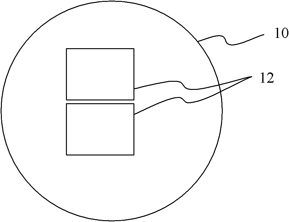
[0038] S10, providing a detection sample, the detection sample has at least two regions to be detected, that is, a first region to be detected and a second region to be detected;

[0039] S20, forming a mark on the first region to be detected of the detection sample;

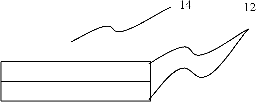
[0040] S30, cutting out a first sample from the first area to be detected, the first sample including the mark, cutting out a second sample from the second area to be detected, the shape of the second sample and The shape of the first sample is the same;

[0041] S40, adhering one side of the first sample and the second sample with the area to be detected is bonded to form a double sample;

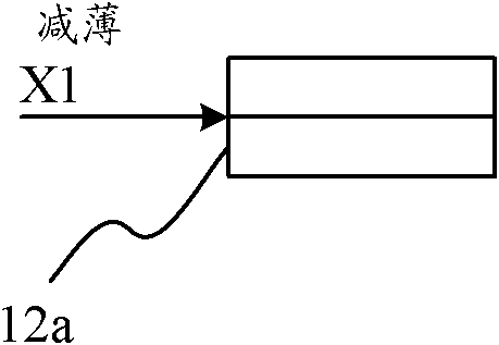
[0042] S50, thinning the double swatch along two opposite sides of the cut swatch until the mark is exposed.


PUM

PropertyMeasurementUnit
lengthaaaaaaaaaa
depthaaaaaaaaaa
widthaaaaaaaaaa

Abstract

The invention relates to a preparation method for a transmission electron microscope (TEM) sample. The method comprises the following steps: providing a sample requiring detection, wherein the sample requiring detection has at least two areas requiring detection, and the two areas comprises a first detection area and a second detection area; forming a mark on the first detection area of the sample requiring detection; carrying out cutting for the first detection area to obtain a first sample sheet, and carrying out cutting for the second detection area to obtain a second sample sheet, wherein the first sample sheet comprises the mark, and the shape of second sample sheet is the same as the shape of the first sample sheet; attaching and bonding the surface of the first sample sheet and the surface of the second sample sheet to form a two-sample sheet, wherein the surface of the first sample sheet and the surface of the second sample sheet have the areas requiring detection; carrying out milling for the two-sample sheet along the two cut relative side surfaces of the two-sample sheet until the mark is exposed, such that the TEM analysis can be performed for any areas of the sample requiring detection.

Description

technical field [0001] The invention relates to the technical field of semiconductor manufacturing, in particular to the field of sample preparation methods for TEM (Transmission Electron Microscope). Background technique [0002] In the semiconductor manufacturing industry, there are a variety of inspection equipment, among which EM is an important tool for inspecting the morphology, size and characteristics of the thin films that make up the device. Commonly used EMs include TEM (Transmission Electron Microscope) and SEM (Scanning Electron Microscope). The working principle of TEM is to thin the sample to be tested by cutting, grinding, ion thinning, etc., and then put it into the TEM observation room, irradiate the sample with a high-voltage accelerated electron beam, enlarge the shape of the sample, and project it on the screen. One of the outstanding advantages of TEM is that it has a high resolution and can observe the shape and size of extremely thin films. [0003]...

Claims


Application Information

Patent Timeline
Patent Type & Authority Patents(China)
IPC IPC(8): G01N1/28
Inventor 段淑卿杨卫明芮志贤陆冠兰
Owner SEMICON MFG INT (SHANGHAI) CORP
Why Eureka
Try Eureka