Unlock instant, AI-driven research and patent intelligence for your innovation.

Method for detecting small delay defects

A defect, test mode technology, applied in the direction of measuring electricity, measuring devices, measuring electrical variables, etc., can solve the problems of increasing the number of modes and running time, and reducing the actual performance of time-aware ATPG methods.

Active Publication Date: 2012-05-23
TAIWAN SEMICON MFG CO LTD
View PDF4 Cites 4 Cited by
  • Summary
  • Abstract
  • Description
  • Claims
  • Application Information

AI Technical Summary

Problems solved by technology

However, as the IC part size grows, the number of modes and run times can grow exponentially
This may degrade the actual performance of time-aware ATPG methods

Method used


Image

  • Method for detecting small delay defects
  • Method for detecting small delay defects
  • Method for detecting small delay defects

Examples


Embodiment Construction

[0021] The making and using of various embodiments of the invention are discussed in detail below. It should be appreciated, however, that the present invention provides many applicable concepts that can be implemented in a wide variety of specific contexts. The specific embodiments discussed are merely illustrative of specific ways to make and use the invention, and do not limit the scope of the invention.

[0022] The present invention will be described according to a preferred embodiment in the specification, that is, a test pattern generation technique for detecting small delay defects (SDDs) will be described. However, the present invention is also applicable to various test pattern generation techniques for many other types of defects.

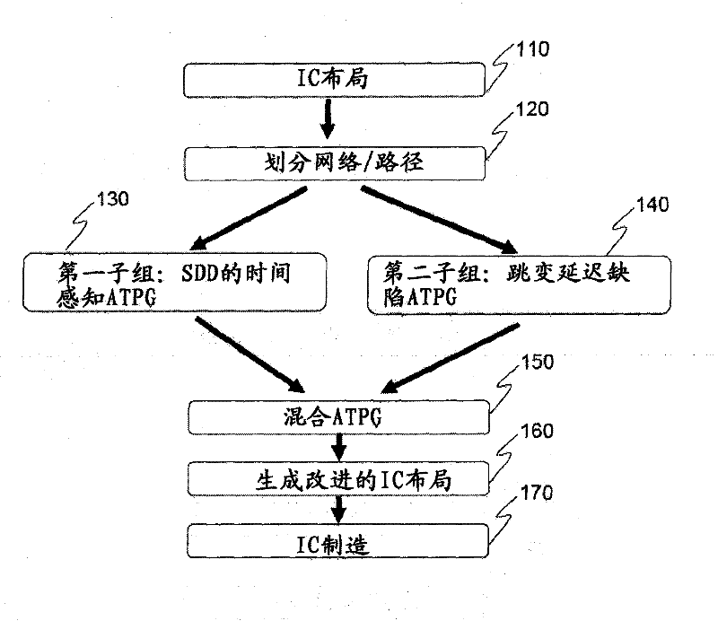
[0023] first, figure 1 What is involved is a flow chart of generating a test pattern for detecting small delay defects (SDD) based on a physics-aware automatic test pattern generation (ATPG) method. In step 110, a physically aware ATP...


PUM


Abstract

System and method for effectively detecting small delay defects is disclosed. The method first loads layout information of an integrated circuit. Then, the nets and paths of the integrated circuit are partitioned into two groups based upon their physical information. The physical information comprises the length of each path and net and the number of vias at each path and net. A timing-aware automatic test pattern generator is configured to generate test patterns for the first group having paths and nets susceptible to small delay defects. A traditional transition delay fault test pattern generator is configured to generate test patterns for the second group.

Description

technical field [0001] The invention relates to the field of semiconductor design, and more particularly, to a detection method for small delay defects. Background technique [0002] Advances in semiconductor design methods and manufacturing processes have resulted in ever-increasing complexity of integrated circuits (ICs). Modern ICs no longer just include multiple transistors, but also operate at higher clock frequencies. These advances, such as higher clock frequencies, make modern ICs more susceptible to timing-related defects such as small delay defects (SDD). However, since IC designers may design ICs according to the timing specification of the IC itself, some ICs may not always be able to undergo SDD testing due to process variations and manufacturing defects. Therefore, testing of SDD is an important step to separate defective chips from non-defective chips. [0003] SDD includes small delay variations that occur in ICs due to semiconductor manufacturing process ...

Claims


Application Information

Patent Timeline
Patent Type & Authority Applications(China)
IPC IPC(8): G06F17/50
CPCG01R31/318328
Inventor 桑迪·库马·戈埃尔沙鲁巴·古普塔张简维平刘钦洲
Owner TAIWAN SEMICON MFG CO LTD