Printed circuit board, tinning line thereof and tinning method thereof

A printed circuit board and circuit technology, applied in the field of microelectronics, can solve problems such as large heat generation, uneven tinning, and circuit burnout.

Active Publication Date: 2012-05-23
FOSHAN SHUNDE HAIER INTELLIGENT ELECTRONICS CO LTD
View PDF6 Cites 3 Cited by
  • Summary
  • Abstract
  • Description
  • Claims
  • Application Information

AI Technical Summary

Problems solved by technology

like figure 1 As shown, the PCB soldering line 1 provided by the prior art is not tinned or a wide tin strip is used to directly run through the entire soldering line 1. When the wave soldering process is performed, it is easy to cause uneven tinning, and in some places Thick, some places are thin, and in the case of high current, the thin place generates a lot of heat, which makes the temperature rise of the whole PCB higher, which is not conducive to heat dissipation, causing safety hazards; and, at the junction of the tin-hanging line and the component pad place, such as figure 1 As s

Method used


Image

  • Printed circuit board, tinning line thereof and tinning method thereof
  • Printed circuit board, tinning line thereof and tinning method thereof
  • Printed circuit board, tinning line thereof and tinning method thereof

Examples


Embodiment 1

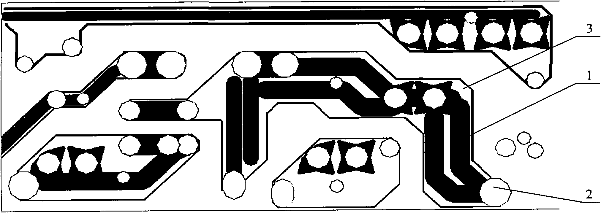
[0028] The embodiment of the present invention provides a printed circuit board tin hanging circuit 1, such as figure 2 As shown, the tin hanging circuit 1 includes several evenly distributed tin hanging bars 11, which are independent of each other and do not touch each other.

[0029] Because the solder is flowing, the existing wide tin-strip tin hanging circuit 1, during the wave soldering process, the solder will move along the slope direction of the tin hanging, resulting in less tin in the component pad 2, which affects the soldering firmness At the same time, the tin-hanging line 11 is not full and uniform enough, which will eventually affect the quality of the tin. Therefore, in order to avoid uneven tin loading caused by the flow of solder, the tin hanging circuit 1 is set to a structure where the tin hanging bars 11 are evenly distributed. The hanging tin bars 11 are independent of each other and do not touch each other. The solder on each hanging tin bar 11 is only It ...

Embodiment 2

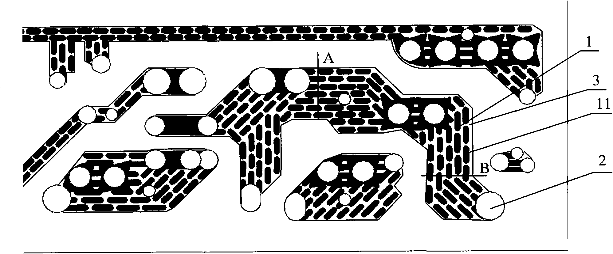
[0035] The embodiment of the present invention provides a printed circuit board, such as figure 2 As shown, it includes: a tin hanging circuit 1 which includes a number of evenly distributed tin hanging bars 11, and the tin hanging bars 11 are independent of each other and do not touch each other.

[0036] Wherein, in order to enhance current carrying and heat dissipation, the long side of the tin hanging bar 11 is parallel to the direction of the tin hanging line 1, and several hanging tin bars 11 are staggered, so that the tin hanging area of ​​the cross section of the entire tin hanging line 1 is maintained Consistent, so that the current carrying current of the whole hanging tin circuit 1 is consistent.

[0037] The structure of the tin-hanging circuit 1 in this embodiment is completely the same as the foregoing embodiment, and will not be repeated here.

[0038] In the technical solution of this embodiment, by setting the tin hanging circuit 1 of the printed circuit board as a ...

Embodiment 3

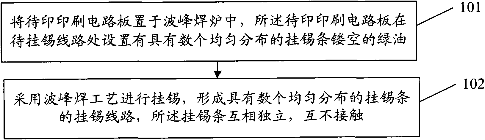
[0040] The embodiment of the present invention provides a tin hanging method, such as image 3 As shown, the method includes:

[0041] Step 101: Place the printed circuit board to be printed in a wave soldering furnace, and the printed circuit board to be printed is provided with a number of evenly distributed tin hanging strips hollowed out green oil at the line to be tinned;

[0042] Step 102: Perform tin hanging by using a wave soldering process to form a tin hanging circuit with a number of evenly distributed tin hanging bars, which are independent of each other and do not touch each other.

[0043] Wherein, the long sides of the formed tin hanging bar are parallel to the direction of the tin hanging line, and the tin hanging bars are arranged in a staggered manner, so that the tin hanging area of ​​the cross section on the entire tin hanging line remains consistent.

[0044] In the technical solution of this embodiment, a printed circuit board to be printed with a number of evenl...


PUM

PropertyMeasurementUnit
Lengthaaaaaaaaaa
Widthaaaaaaaaaa

Abstract

An embodiment of the invention discloses a printed circuit board, a tinning line thereof and a tinning method thereof, relating to the microelectronic technology field, and welding looseness and tinning unevenness caused by soldering tin mobility can be avoided. The printed circuit board tinning line comprises a plurality of tinning strips which are uniformly distributed. The tinning strips are mutually independent and do no contact each other. The printed circuit board, the tinning line and the tinning method are applied to printing of the printed circuit board.

Description

Technical field [0001] The invention relates to the field of microelectronics, in particular to a printed circuit board and its tin hanging circuit and tin hanging method. Background technique [0002] In the manufacturing process of a printed circuit board (PCB), generally, a wave soldering process is used for hanging tin. [0003] Wave soldering is to make the soldering surface of the plug-in board directly contact the high-temperature liquid tin to achieve the purpose of soldering. The high-temperature liquid tin maintains a slope, and a special device makes the liquid tin form a wave-like tin hanging circuit. Such as figure 1 As shown, the PCB tin hanging circuit 1 provided by the prior art is not tin hanging or a wide tin strip is used to directly penetrate the whole tin hanging circuit 1. During the wave soldering process, it is easy to cause uneven tin application, and in some places Thick, thin in some places, but in the case of high current, the thin place generates a lot...

Claims


Application Information

Patent Timeline
IPC IPC(8): H05K3/34H05K1/02
Inventor 高延飞
Owner FOSHAN SHUNDE HAIER INTELLIGENT ELECTRONICS CO LTD
Why Eureka
Try Eureka