
Method and system of grain detecting

A detection method and grain technology, applied in the direction of measuring electricity, measuring devices, measuring electrical variables, etc., can solve the problem that the grain cannot be in contact with the probe accurately, so as to solve the problem of different sizes of needle marks, ensure contact, prevent The effect of very small needle marks

Active Publication Date: 2012-06-13
SHENZHEN SIDEA SEMICON EQUIP
View PDF5 Cites 7 Cited by
  • Summary
  • Abstract
  • Description
  • Claims
  • Application Information

AI Technical Summary

Problems solved by technology

[0004] In order to solve the technical problem that the grain cannot be in contact with the probe accurately, the invention provides a grain detection method

Method used


Image

  • Method and system of grain detecting
  • Method and system of grain detecting
  • Method and system of grain detecting

Examples


Embodiment Construction

[0030] Specific embodiments of the present invention will be described in further detail below in conjunction with the accompanying drawings.

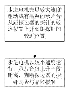
[0031] Such as figure 1 Shown, the specific embodiment of a kind of grain detecting method, comprises the following steps:

[0032] A. The stepper motor first drives the wafer stage loaded with crystal grains at a higher speed to rise from a position farther away from the probe of the edge detector to a position closer to the probe;

[0033] B. The stepping motor runs at a small speed, and every time the wafer table rises for a certain distance, it is judged whether the probe of the edge detector is in contact with the die.

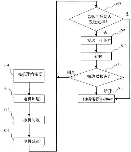
[0034] Such as figure 2 As shown, a more specific embodiment of a grain detection method:

[0035] S04. The stepper motor starts to run, driving the wafer carrier loaded with crystal grains to rise;

[0036] S05-S07. After the stepper motor has gone through three stages of acceleration, constant speed and dec...


PUM


Abstract

The invention discloses a method and a system of grain detecting. The method includes the following steps, A, a stepping motor drives a grain-borne piece bearing table to rise from a position farer from a feeler pin of an edge feeler to a position nearer to the feeler pin at a higher speed; and B, as the stepping motor operates at a lower speed, once the piece bearing table rises for a certain distance, and feeler pin of the edge feeler is judged to be contacted with the grain or not. The piece bearing table can operate at a higher speed so as to enable the detection of the grain to be completed within a shorter time, ensure the precise and reliable contact of the grain and the feeler pin, and ensure the sizes of the pin traces on the grain to be rather identical; the uncertainty that the sizes of the pin traces left on the grain when the feeler pin is contacted with the grain are different as the grain is driven to vibrate due to the fact that the stepping motor is easy to vibrate is avoided; and the technical problem that the pin traces are different as the planeness and the precision are not high is solved.

Description

technical field [0001] The invention relates to the field of semiconductor detection, in particular to a crystal grain detection method and system. Background technique [0002] The main function of the LED probe station is to move the position of the die during the process of testing the LED die. The whole machine includes the positioning of X, Y, Z, three-axis space, and the control of the angle of the wafer by the θ axis. The four-axis motion of the probe station ensures reliable die-to-probe contact during testing. After the current die is tested, quickly switch to the next die. [0003] The traditional probe station uses a fixed step to control the motion of the Z axis. Each time the wafer on the wafer carrier on the probe station is set to a fixed height, it rises until the probe touches the grain electrode. However, due to the difference in the flatness of the entire wafer and the flatness of the wafer holder, the height of different chips will have a difference of...

Claims


Application Information

Patent Timeline
IPC IPC(8): G01R31/26G01R1/067
Inventor 杨波齐岳
Owner SHENZHEN SIDEA SEMICON EQUIP
Learn More