One-time programmable memory and manufacturing method

A manufacturing method and memory technology, which are applied in the manufacturing of semiconductor/solid-state devices, electric solid-state devices, semiconductor devices, etc., can solve the problems of decreased data retention, affecting the threshold voltage of floating gate 11, charge loss, etc., so as to reduce the charge loss. the probability of increased data retention, the effect of reducing requirements

Active Publication Date: 2016-06-08
SHANGHAI HUAHONG GRACE SEMICON MFG CORP
View PDF6 Cites 0 Cited by
  • Summary
  • Abstract
  • Description
  • Claims
  • Application Information

AI Technical Summary

Problems solved by technology

However, the distance d between the plug 12 and the floating gate 11 is getting smaller and smaller, and the reduction of the distance d will cause the charge in the floating gate 11 to be lost through the plug 12, thereby affecting the performance of the floating gate 11. Threshold voltage, which in turn causes a decline in OTP's data retention (DataRetention)

Method used


Image

  • One-time programmable memory and manufacturing method
  • One-time programmable memory and manufacturing method
  • One-time programmable memory and manufacturing method

Examples


Embodiment Construction

[0032] In order to make the above objects, features and advantages of the present invention more comprehensible, specific implementations of the present invention will be described in detail below in conjunction with the accompanying drawings.

[0033] In the following description, many specific details are set forth in order to fully understand the present invention, but the present invention can also be implemented in other ways than those described here, so the present invention is not limited by the specific embodiments disclosed below.

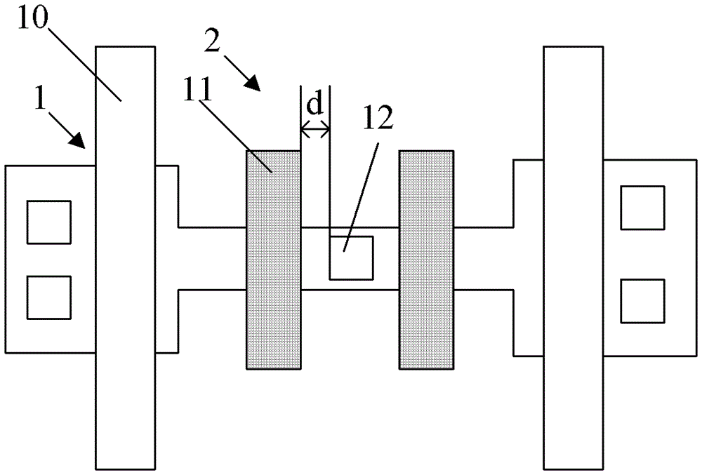
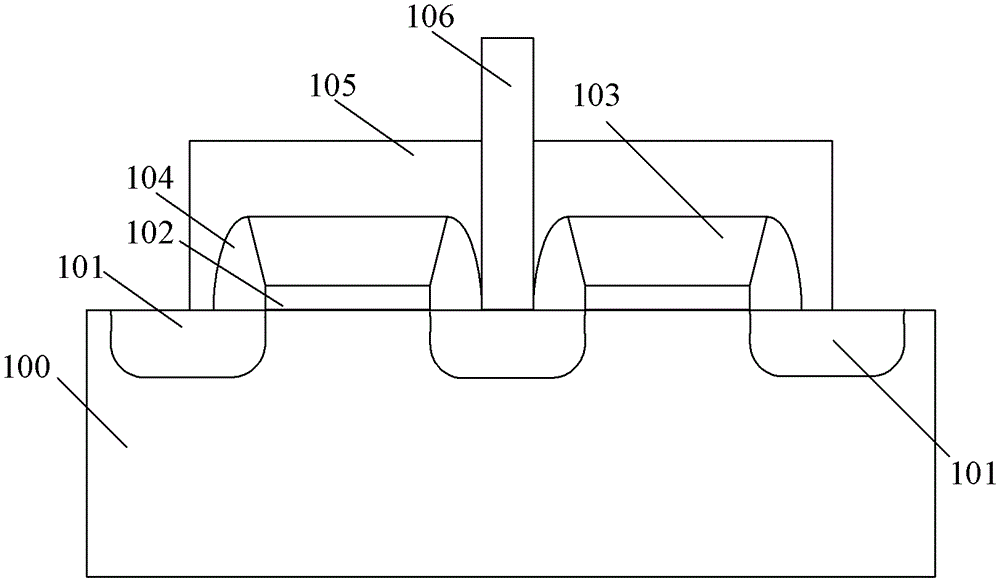
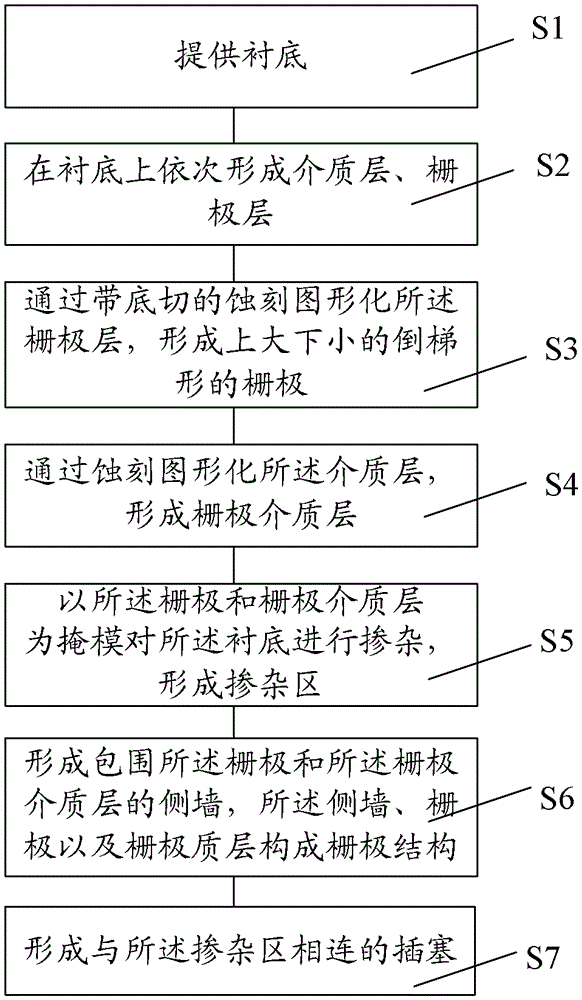
[0034] In order to solve the problems in the prior art, the present invention provides a one-time programmable memory, which includes a plurality of storage units, the storage units include a read MOS transistor, and the read MOS transistor includes a floating gate , the floating gate is an inverted trapezoidal structure with a large top and a small bottom.

[0035] In the present invention, the floating gate is an inverted trapezoidal st...


PUM


Abstract

A one-time programmable memory and its manufacturing method, the one-time programmable memory includes a plurality of storage units, the storage units include a control MOS transistor and a read MOS transistor connected in series, the read MOS transistor includes a floating gate, the The floating gate is an inverted trapezoidal structure with a large top and a small bottom. The storage unit includes a control MOS transistor and a read MOS transistor connected in series, and the steps of manufacturing the read MOS transistor include: providing a substrate; sequentially forming a dielectric layer and a gate layer on the substrate; etching with an undercut patterning the gate layer to form an inverted trapezoidal gate with a large top and a small bottom; patterning the dielectric layer by etching to form a gate dielectric layer; using the gate and the gate dielectric layer as a mask to Doping the substrate to form a doped region; forming a side wall surrounding the gate and the gate dielectric layer, and the side wall, the gate and the gate dielectric layer constitute a gate structure. The invention can improve the data retention of the one-time programmable memory.

Description

technical field [0001] The invention relates to the technical field of semiconductors, in particular to a one-time programmable memory and a manufacturing method. Background technique [0002] A one-time programmable memory (One Time Programable, OTP) is one of common memories, and after information is written in the OTP, the information cannot be changed again. Because the manufacturing process of OTP is relatively simple, the cost is low, and OTP also has certain flexibility at the same time, so the application of OTP is relatively extensive. [0003] Based on different OTP structures, the OTP is divided into coupling capacitor type, series transistor type, dielectric breakdown type and the like. [0004] refer to figure 1 , shows a schematic structural diagram of an embodiment of the prior art OTP. The OTP is an example of a series transistor type OTP. The OTP includes a plurality of storage units, and each storage unit includes two NMOS transistors connected in series...

Claims


Application Information

Patent Timeline
Patent Type & Authority Patents(China)
IPC IPC(8): H01L27/115H01L21/8247
Inventor 令海阳吴小利
Owner SHANGHAI HUAHONG GRACE SEMICON MFG CORP
Why Eureka
Try Eureka