Tunneling insulating layer, flash memory device including the same, memory card and system including the flash memory device, and methods of manufacturing the same

a technology of insulating layer and insulating layer, which is applied in the direction of solid-state devices, semiconductor/solid-state device details, instruments, etc., can solve the problems of data retention reduction, program/erase operation speed of flash memory devices may decrease, and data retention may be reduced, so as to improve data retention, improve reliability and manufacturing methods, and increase program/erase operation speed

Inactive Publication Date: 2009-05-28
SAMSUNG ELECTRONICS CO LTD
View PDF4 Cites 29 Cited by
  • Summary
  • Abstract
  • Description
  • Claims
  • Application Information

AI Technical Summary

Benefits of technology

[0012]Example embodiments provide a tunneling insulating layer and a flash memory device including the same that may increase a program / erase operation speed and may have improved data retention so as to improve reliability and methods of manufacturing the same. Example embodiments also provide a memory card and system including the flash memory device and methods of manufacturing the same.

Problems solved by technology

Consequently, program and erase operation speeds of flash memory devices may decrease.
However, data retention may be reduced due to an increase in leakage current.
On the other hand, when the tunneling insulating layer is formed relatively thick, a program / erase operation speed of the flash memory device may decrease.

Method used


Image

  • Tunneling insulating layer, flash memory device including the same, memory card and system including the flash memory device, and methods of manufacturing the same
  • Tunneling insulating layer, flash memory device including the same, memory card and system including the flash memory device, and methods of manufacturing the same
  • Tunneling insulating layer, flash memory device including the same, memory card and system including the flash memory device, and methods of manufacturing the same

Examples


Embodiment Construction

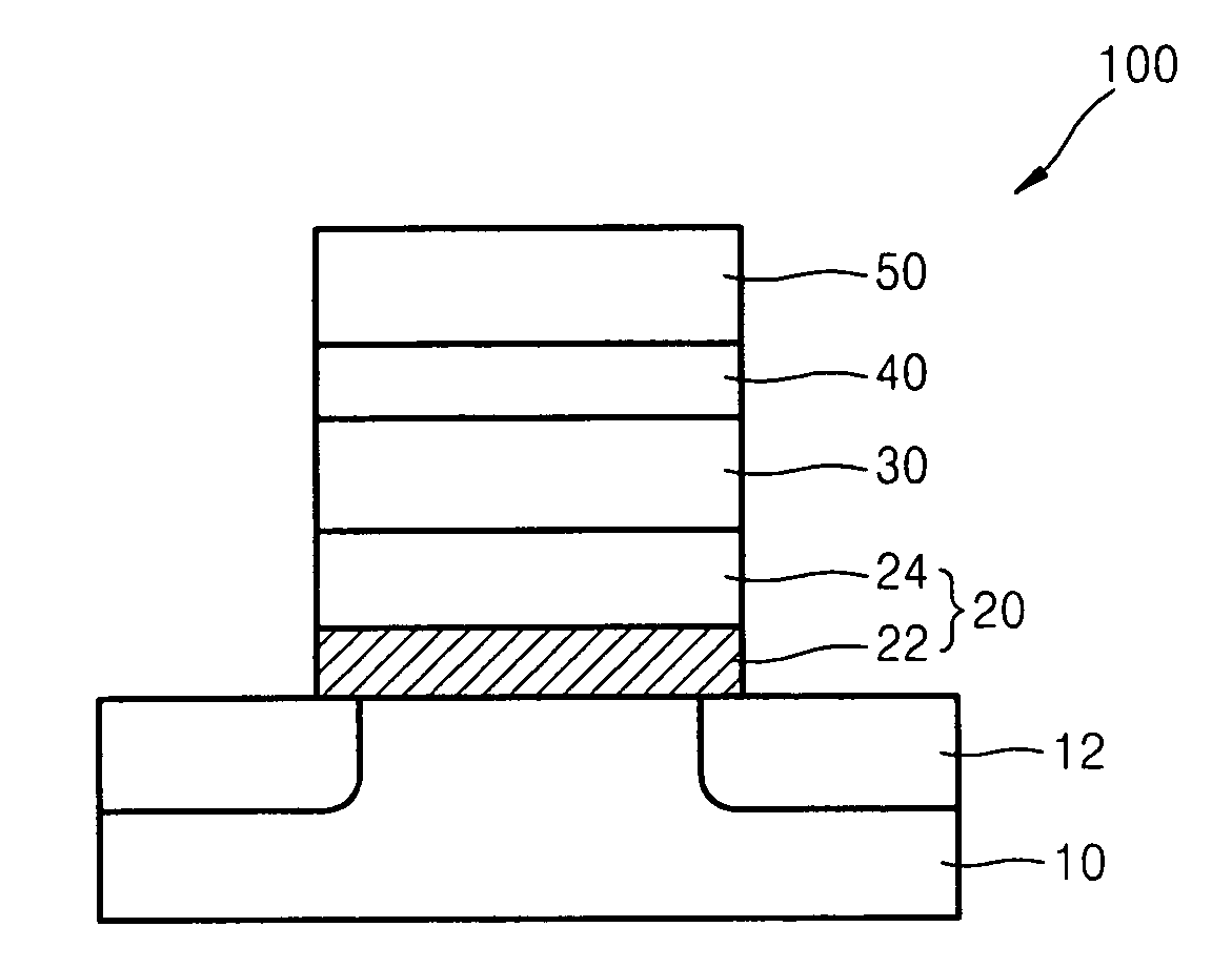
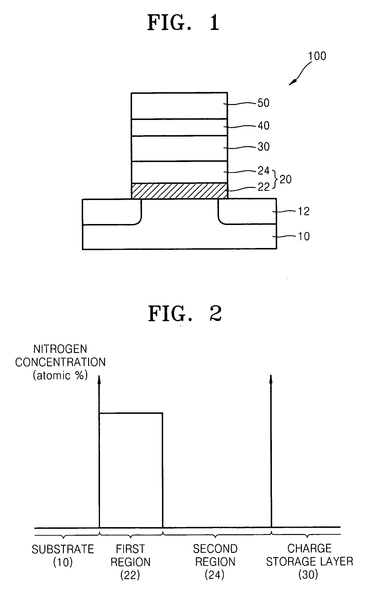
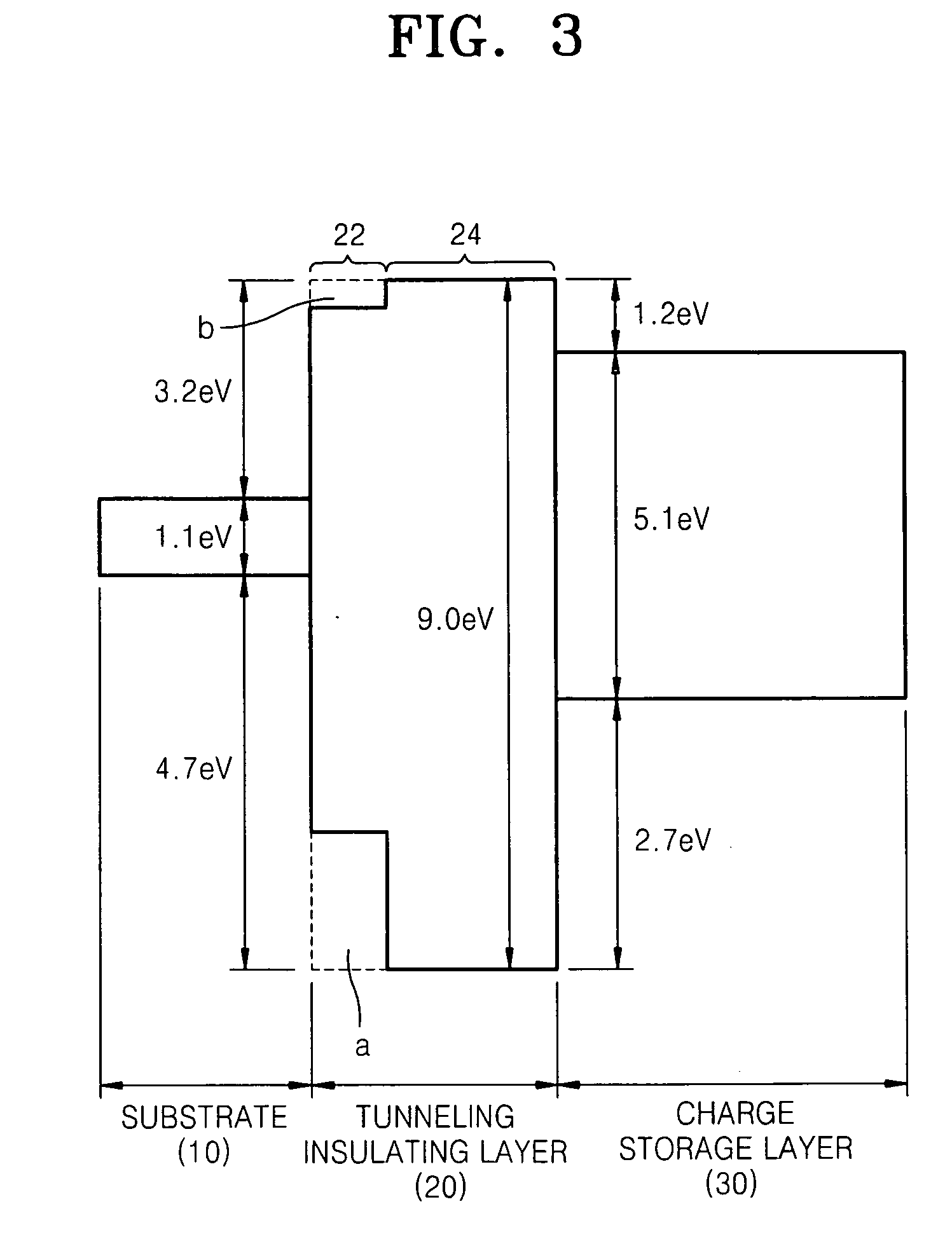
[0035]Reference will now be made in detail to example embodiments, examples of which are illustrated in the accompanying drawings. However, example embodiments are not limited to the embodiments illustrated hereinafter, and the embodiments herein are rather introduced to provide easy and complete understanding of the scope and spirit of example embodiments. In the drawings, the thicknesses of layers and regions are exaggerated for clarity.

[0036]It will be understood that when an element, such as a layer, a region, or a substrate, is referred to as being “on,”“connected to” or “coupled to” another element, it may be directly on, connected or coupled to the other element or intervening elements may be present. In contrast, when an element is referred to as being “directly on,”“directly connected to” or “directly coupled to” another element or layer, there are no intervening elements or layers present. Like reference numerals refer to like elements throughout. As used herein, the term ...


PUM


Abstract

Provided is a tunneling insulating layer, a flash memory device including the same that increases a program / erase operation speed of the flash memory device and has improved data retention in order to increase reliability of the flash memory device, a memory card and system including the flash memory device, and methods of manufacturing the same. A tunneling insulating layer may include a first region and a second region on the first region, wherein the first region has a first nitrogen atomic percent, the second region has a second nitrogen atomic percent, and the second nitrogen atomic percent is less than the first nitrogen atomic percent. The flash memory device according to example embodiments may include a substrate including source and drain regions and a channel region between the source and drain regions, the tunneling insulating layer on the channel region, a charge storage layer on the tunneling insulating layer, a blocking insulation layer on the charge storage layer, and a gate electrode on the blocking insulation layer.

Description

PRIORITY STATEMENT[0001]This application claims priority under U.S.C. §119 to Korean Patent Application No. 10-2007-0121998, filed on Nov. 28, 2007, in the Korean Intellectual Property Office (KIPO), the entire contents of which are incorporated herein by reference.BACKGROUND[0002]1. Field[0003]Example embodiments relate to a tunneling insulating layer, a flash memory device including the same, a memory card and a system including the flash memory device, and methods of manufacturing the same. Other example embodiments relate to a tunneling insulating layer, a flash memory device that may increase a program / erase operation speed of the flash memory device and has improved data retention, a memory card and a system including the flash memory device, and methods of manufacturing the same.[0004]2. Description of the Related Art[0005]Among semiconductor memory devices, non-volatile memory devices retain stored data even if the power supply is interrupted. In recent years, owing to the i...

Claims


Application Information

Patent Timeline
Patent Type & Authority Applications(United States)
IPC IPC(8): H01L29/788
CPCG11C16/0416H01L21/28273H01L21/28282H01L29/792H01L29/4234H01L29/513H01L29/7881H01L29/42324H01L29/40114H01L29/40117H10B99/00
Inventor KIM, CHUL-SUNGCHOI, SI-YOUNGKOO, BON-YOUNGHWANG, KI-HYUNNOH, YOUNG-JIN
Owner SAMSUNG ELECTRONICS CO LTD
Why Eureka
Try Eureka