Semiconductor device and manufacturing method thereof

a semiconductor and integrated circuit technology, applied in semiconductor devices, digital storage, instruments, etc., can solve problems such as large power consumption, deterioration of transistors, and significant problems, and achieve the effects of reducing power consumption, suppressing short-channel effects, and improving data retention characteristics of semiconductor memory devices

Active Publication Date: 2014-07-15
SEMICON ENERGY LAB CO LTD
View PDF165 Cites 26 Cited by
  • Summary
  • Abstract
  • Description
  • Claims
  • Application Information

AI Technical Summary

Benefits of technology

[0008]Thus, it is an object of the present invention to provide a technique that can improve data retention characteristics of a semiconductor memory device. Another object is to provide a technique that can reduce power consumption as well as improving data retention characteristics of a semiconductor memory device.
[0021]Improvement of data retention characteristics of a semiconductor memory device can be achieved. A reduction of power consumption as well as improvement of data retention characteristics of a semiconductor memory device can be achieved.

Problems solved by technology

However, a conventional DRAM needs to be refreshed at an interval of several tens of milliseconds to hold data, which results in large power consumption.
In addition, a transistor therein is frequently turned on and off; thus, deterioration of the transistor is also a problem.
These problems become significant as the memory capacity increases and transistor miniaturization advances.

Method used


Image

  • Semiconductor device and manufacturing method thereof
  • Semiconductor device and manufacturing method thereof
  • Semiconductor device and manufacturing method thereof

Examples


embodiment 1

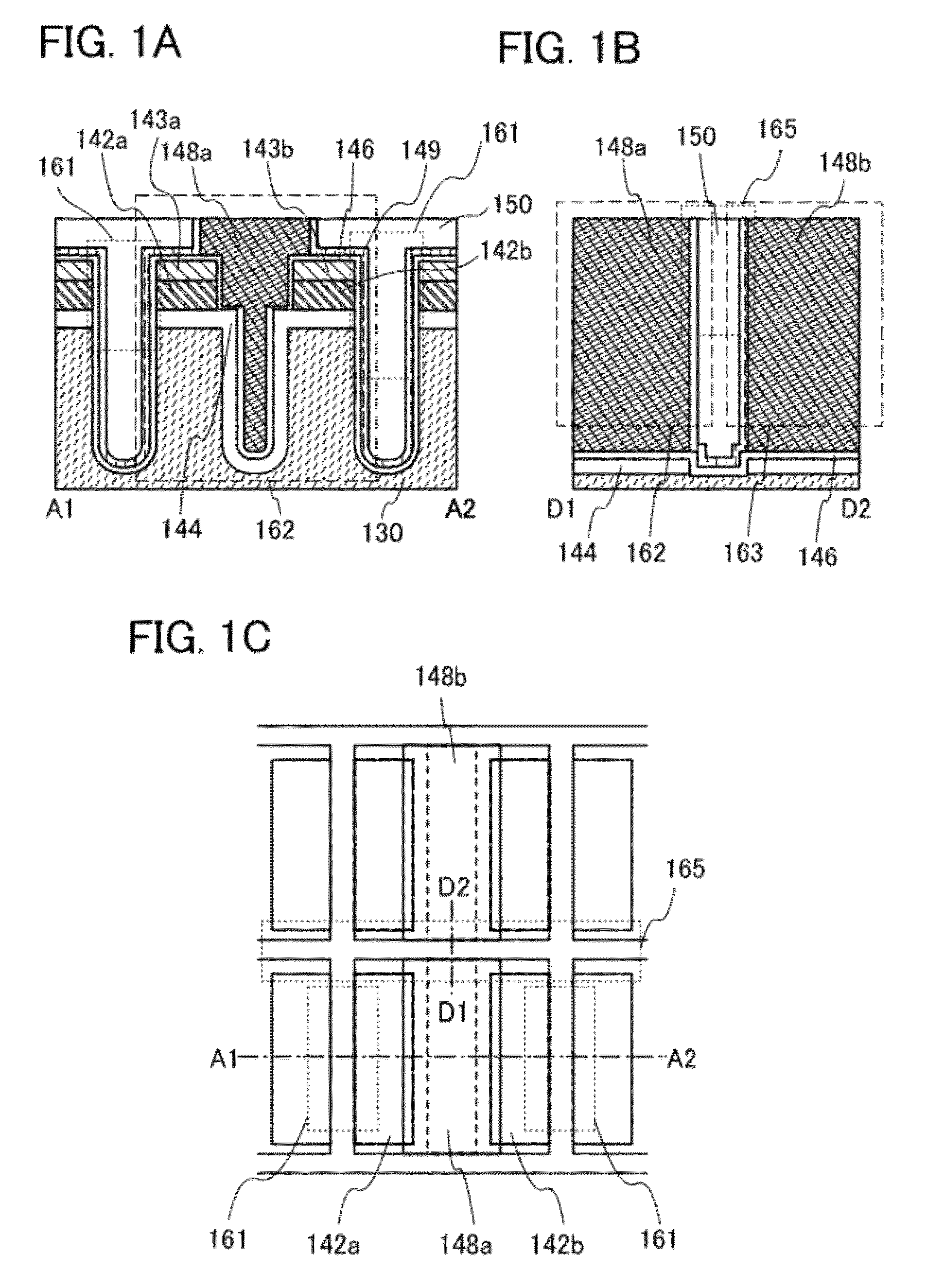
[0036]In this embodiment, a structure of a transistor and a method for manufacturing the transistor according to one embodiment of the present invention will be described with reference to FIGS. 1A to 1C and FIGS. 2A to 2C. FIG. 1A is an example of a cross-sectional view of a transistor 162 in a channel-length direction. FIG. 1B is an example of a cross-sectional view perpendicular to an element isolation region 165 between the transistor 162 and a transistor 163. FIG. 1C is an example of a top view of the transistor 162 and the transistor 163. Note that FIG. 1B is part of a cross-sectional view of the transistor 162 in a channel-width direction, and corresponds to a cross-sectional view taken along a dotted line D1-D2 in FIG. 1C. FIG. 1A corresponds to a cross-sectional view taken along a dotted line A1-A2 in FIG. 1C.

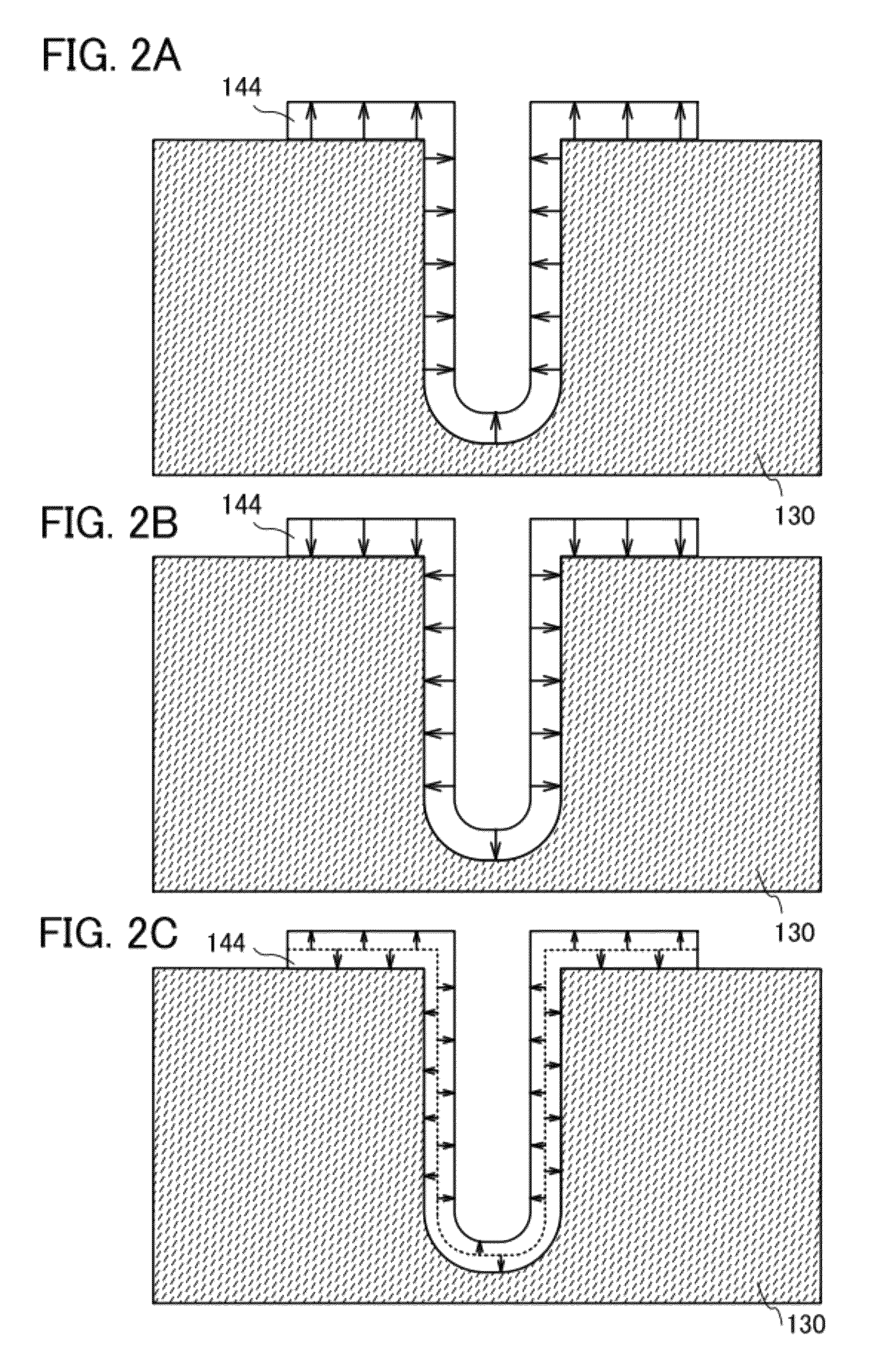
[0037]First, an insulating layer 130 is formed with an oxide film over a semiconductor substrate. Then, a plurality of trenches (also referred to as grooves) is formed...

embodiment 2

[0062]FIGS. 3A and 3B illustrates an example of a semiconductor device which includes the transistor 162 illustrated in FIGS. 1A to 1C, which can hold stored data even when not powered, and which has an unlimited number of write cycles.

[0063]Since the off-state current of the transistor 162 is small, stored data can be held for a long time owing to such a transistor. In other words, the frequency of refresh operation can be extremely lowered, which leads to a sufficient reduction in power consumption.

[0064]FIG. 3A illustrates an example of a cross section of the semiconductor device.

[0065]The semiconductor device illustrated in FIG. 3A includes a transistor 160 including a first semiconductor material in a lower portion, and a transistor 162 including a second semiconductor material in an upper portion. The transistor 162 is the same as that in Embodiment 1; thus, for description of FIGS. 3A and 3B, the same reference numerals are used for the same parts as those in FIG. 1A.

[0066]He...

embodiment 3

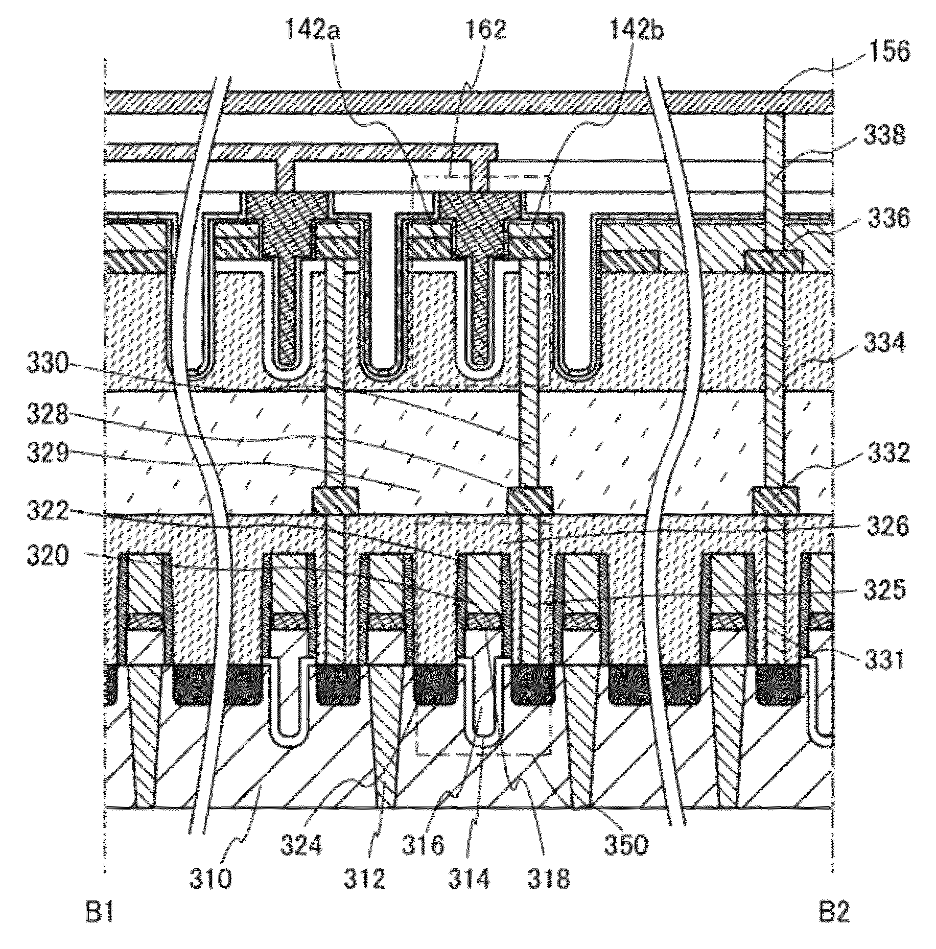
[0081]In this embodiment, a semiconductor device which includes the transistor 162 illustrated in FIGS. 1A to 1C, which can hold stored data even when not powered, which has an unlimited number of write cycles, and which has a structure different from the structure described in Embodiment 2 will be described with reference to FIG. 4.

[0082]The semiconductor device illustrated in FIG. 4 includes a transistor 350 including a first semiconductor material in a lower portion, and a transistor 162 including a second semiconductor material in an upper portion. Although a plurality of transistors is formed using semiconductor materials in the upper and lower portions, the transistor 350 and the transistor 162 will be typically described. Note that FIG. 4 which is taken along line B1-B2 corresponds to a cross-sectional view perpendicular to the channel-length direction of transistors.

[0083]Here, the first semiconductor material and the second semiconductor material are preferably different ma...


PUM


Abstract

A conventional DRAM needs to be refreshed at an interval of several tens of milliseconds to hold data, which results in large power consumption. In addition, a transistor therein is frequently turned on and off; thus, deterioration of the transistor is also a problem. These problems become significant as the memory capacity increases and transistor miniaturization advances. A transistor is provided which includes an oxide semiconductor and has a trench structure including a trench for a gate electrode and a trench for element isolation. Even when the distance between a source electrode and a drain electrode is decreased, the occurrence of a short-channel effect can be suppressed by setting the depth of the trench for the gate electrode as appropriate.

Description

TECHNICAL FIELD[0001]The present invention relates to a technique for miniaturizing semiconductor integrated circuits. The invention disclosed in this specification includes in its scope an element formed using a compound semiconductor, in addition to that formed using a silicon semiconductor, as a component of a semiconductor integrated circuit, and discloses an element formed using an oxide semiconductor as an example.BACKGROUND ART[0002]As semiconductor memory devices, dynamic RAMs (DRAMs) are well-known products and currently used in a variety of electronic devices. A memory cell which is a key component in a DRAM includes a read and write transistor and a capacitor.[0003]Circuit patterns for DRAMs, like those for other semiconductor integrated circuits, have been miniaturized in accordance with the scaling law, and there was a time when it was considered difficult to achieve a design rule of 100 nm or less. One of the reasons is that in a transistor having a channel length of 1...

Claims


Application Information

Patent Timeline
Patent Type & Authority Patents(United States)
IPC IPC(8): H01L29/78
CPCH01L29/22H01L29/7833H01L29/1037H01L29/78H01L27/1225G11C11/403H01L29/4236H01L27/0688H01L27/1156H01L27/108H01L27/1207H01L27/11551H01L29/7827H01L29/7869H10B41/20H10B41/70H10B12/00
Inventor YAMAZAKI, SHUNPEIGODO, HIROMICHI
Owner SEMICON ENERGY LAB CO LTD
Why Eureka
Try Eureka