Method of manufacturing a semiconductor memory with deuterated materials

a semiconductor memory and deuterated material technology, applied in the direction of semiconductor devices, electrical devices, transistors, etc., can solve the problems of reduced data storage density, reduced speed, and higher cost, and reduce the reliability of data, so as to improve data retention and reduce charge loss

Inactive Publication Date: 2005-04-26
INFINEON TECH LLC
View PDF3 Cites 30 Cited by
  • Summary
  • Abstract
  • Description
  • Claims
  • Application Information

AI Technical Summary

Benefits of technology

[0015]The present invention provides a manufacturing method for a MirrorBit® Flash memory and includes providing a semiconductor substrate and successively depositing a first insulating layer, a charge-trapping layer, and a second insulating layer. First and second bitlines are implanted and wordlines are formed before completing the memory. Spacers are formed between the wordlines and an inter-layer dielectric layer is formed over the wordlines. One or more of the second insulating layer, wordlines, spacers, and inter-layer dielectric layer are deuterated, replacing hydrogen bonds with deuterium, thus improving data retention and substantially reducing charge loss.

Problems solved by technology

EEPROM can be easily erased without extra exterior equipment but with reduced data storage density, lower speed, and higher cost.
Unfortunately, this structure inherently requires a great deal of precision in both programming and reading the differences in the levels to be able to distinguish the bits.
The need in the MLS architecture to precisely control the amount of charge in a memory cell while programming also makes the technology slower and the data less reliable.
It also takes longer to access or “read” precise amounts of charge.
A major problem with the MirrorBit architecture has been discovered where the charges, which represent bits of data, tend to drain away over time through the semiconductor device leading to poor data retention.
Many materials used have silicon-hydrogen bonds, which are relatively weak and tend to break, thus leaving large amounts of hydrogen free to act as charge carriers.
A solution to this problem has been long sought but has long eluded those skilled in the art.

Method used


Image

  • Method of manufacturing a semiconductor memory with deuterated materials
  • Method of manufacturing a semiconductor memory with deuterated materials
  • Method of manufacturing a semiconductor memory with deuterated materials

Examples


Embodiment Construction

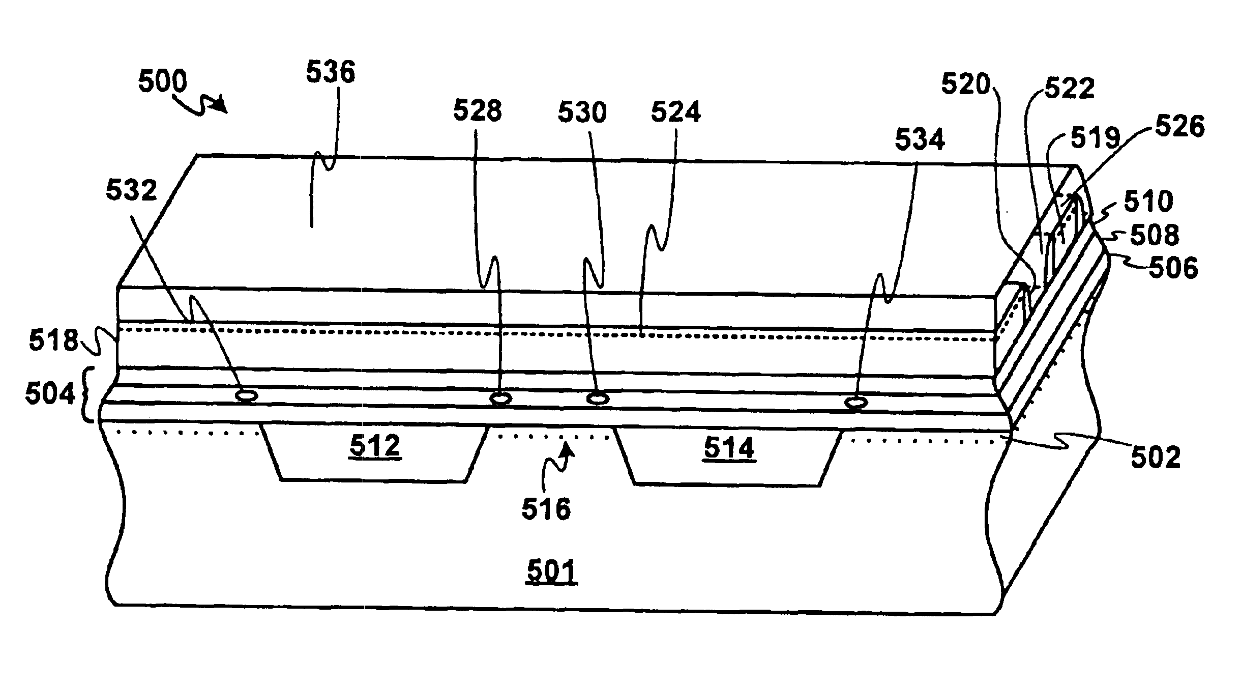
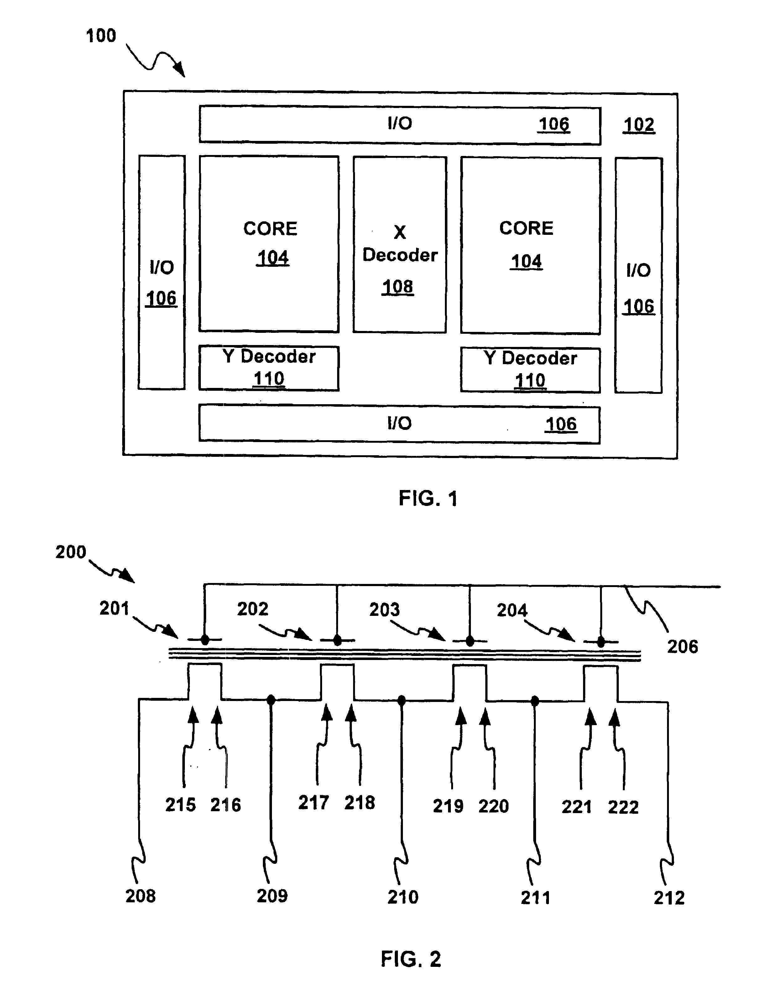
[0023]Referring now to FIG. 1, therein is shown a plan view of a. MirrorBit® Flash EEPROM 100, which commonly includes a semiconductor substrate 102 in which one or more high-density core regions and one or more low-density peripheral portions are formed. High-density core regions typically include one or more M×N array cores 104 of individually addressable, substantially identical MirrorBit Flash memory cells. Low-density peripheral portions typically include input / output (I / O) circuitry and programming circuitry for selectively addressing the individual memory cells. The programming circuitry is represented in part by and includes one or more x-decoders 108 and y-decoders 110, cooperating with I / O circuitry 106 for connecting the source, gate, and drain of selected addressed memory cells to predetermined voltages or impedances to effect designated operations on the memory cell, e.g., programming, reading, and erasing, and deriving necessary voltages to effect such operations.

[0024...


PUM


Abstract

A method for manufacturing a MirrorBit® Flash memory includes providing a semiconductor substrate and successively depositing a first insulating layer, a charge-trapping layer, and a second insulating layer. First and second bitlines are implanted and wordlines are formed before completing the memory. Spacers are formed between the wordlines and an inter-layer dielectric layer is formed over the wordlines. One or more of the second insulating layer, wordlines, spacers, and inter-layer dielectric layers are deuterated, replacing hydrogen bonds with deuterium, thus improving data retention and substantially reducing charge loss.

Description

CROSS REFERENCE TO RELATED APPLICATIONS[0001]This is a divisional of application Ser. No. 10 / 128,771, now U.S. Pat. No. 6,670,241 B1, filed on Apr. 22, 2002, which is incorporated herein by reference thereto.BACKGROUND OF THE INVENTION[0002]1. Technical Field[0003]The present invention relates generally to semiconductor technology and data retention in semiconductor memories.[0004]2. Background Art[0005]Various types of memories have been developed in the past as electronic memory media for computers and similar systems. Such memories include electrically erasable programmable read only memory (EEPROM) and electrically programmable read only memory (EPROM). Each type of memory had advantages and disadvantages. EEPROM can be easily erased without extra exterior equipment but with reduced data storage density, lower speed, and higher cost. EPROM, in contrast, is less expensive and has greater density but lack erasability.[0006]A newer type of memory called “Flash” EEPROM, or Flash mem...

Claims


Application Information

Patent Timeline
Patent Type & Authority Patents(United States)
IPC IPC(8): H01L21/02H01L21/70H01L21/336H01L21/8246
CPCH01L29/66833H01L27/11568H10B43/30
Inventor KAMAL, TAZRIENHALLIYAL, ARVINDNGO, MINH VANRAMSBEY, MARK T.YANG, JEAN Y.SHIRAIWA, HIDEHIKOSUGINO, RINJI
Owner INFINEON TECH LLC
Why Eureka
Try Eureka