Low Power Retention Random Access Memory with Error Correction on Wake-Up

a random access memory and wake-up technology, applied in the field of solid-state memory, can solve the problems of increasing test time, increasing power consumption during operation, and complicating the routing of conductors in the integrated circuit realization, so as to reduce power consumption in data retention mode

Active Publication Date: 2012-12-20
TEXAS INSTR INC
View PDF4 Cites 28 Cited by
  • Summary
  • Abstract
  • Description
  • Claims
  • Application Information

AI Technical Summary

Benefits of technology

[0015]Embodiments of this invention provide a memory and a method of operating the same i

Problems solved by technology

However, increasing the granularity of the retention domains to minimize retention power consumption (i.e., by enabling lower retention power supply voltage levels where possible) increases the chip area required for the memory resources, increases test time, complicates the routing of conductors in the integrated circuit realization, and can increase power consumption during operation.
However, this physical scaling of device sizes does not ne

Method used


Image

  • Low Power Retention Random Access Memory with Error Correction on Wake-Up
  • Low Power Retention Random Access Memory with Error Correction on Wake-Up
  • Low Power Retention Random Access Memory with Error Correction on Wake-Up

Examples


Embodiment Construction

[0026]This invention will be described in connection with its embodiments, namely as implemented into a static random access memory (SRAM) architecture, for example as embedded within a larger-scale integrated circuit, because it is contemplated that the invention is beneficial when utilized in such an application. However, it is also contemplated that embodiments of this invention can provide important and significant advantages if applied to other types of read / write solid-state memory, and to such memory when implemented as stand-alone integrated circuits or embedded in other architectures. Accordingly, it is to be understood that the following description is provided by way of example only, and is not intended to limit the true scope of this invention as claimed.

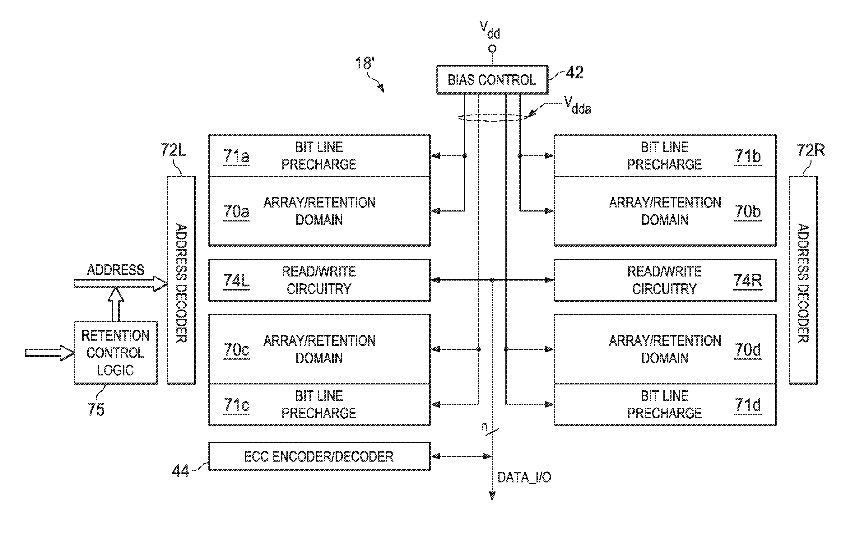
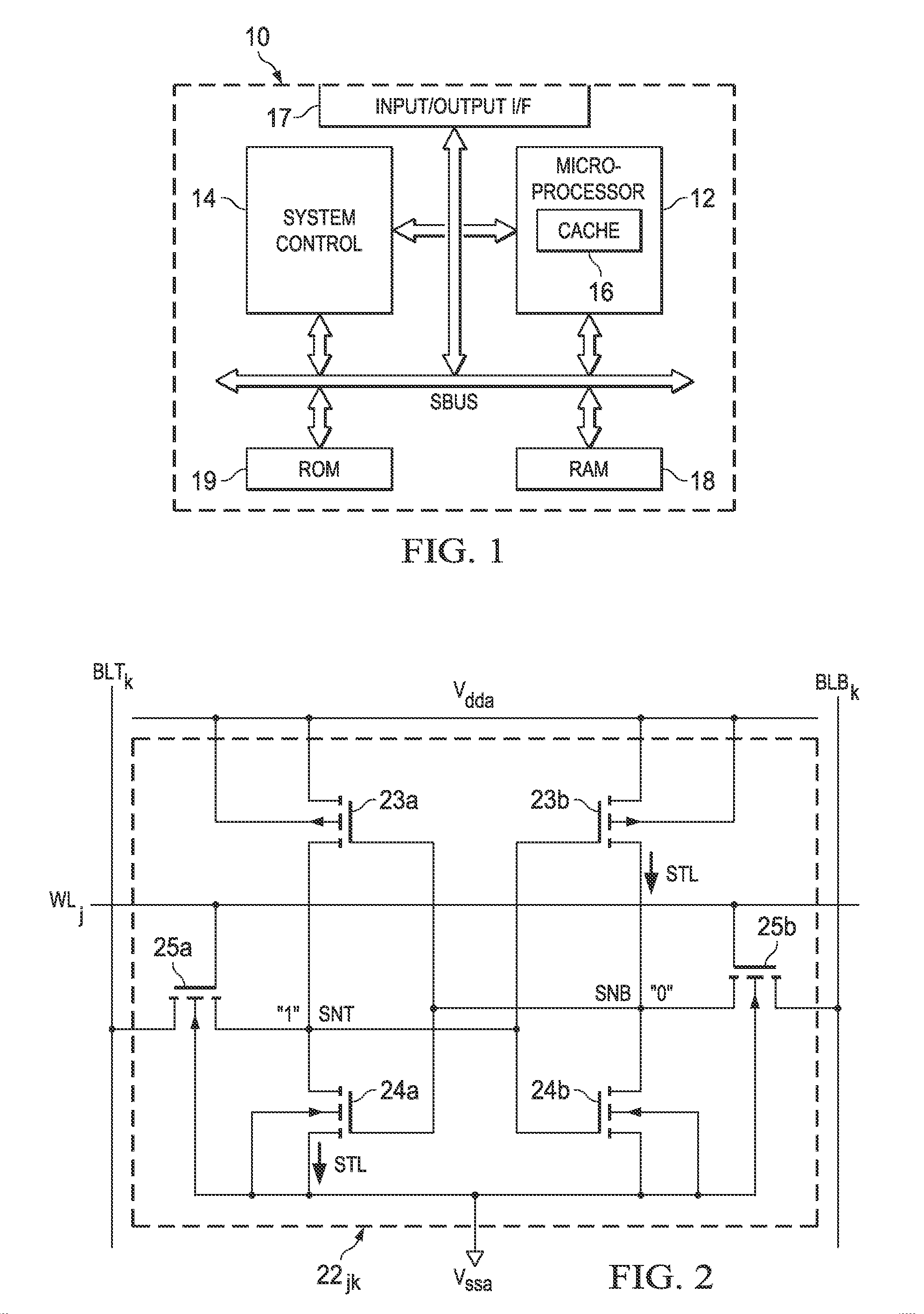
[0027]FIG. 1 illustrates an example of large-scale integrated circuit 10, in the form of a so-called “system-on-a-chip” (“SoC”), as now popular in many electronic systems. Integrated circuit 10 is a single-chip integrate...


PUM


Abstract

Solid-state random access memory including error correction capability applied to memory arrays entering and exiting a data retention mode. Error correction coding of the data to be retained is performed upon determining that a portion of the memory is to enter data retention mode; the parity bits (i.e., bits in addition to those required for storage of the payload) are stored in available memory cells within or external to the retention domain. Upon exit from retention mode, the code words are decoded to correct any errors, and the payload data are returned to the original cells. Error correction encoding and decoding is not performed in the normal operating mode.

Description

CROSS-REFERENCE TO RELATED APPLICATIONS[0001]This application claims priority, under 35 U.S.C. §119(e), of Provisional Application No. 61 / 498,439, filed Jun. 17, 2011; and of Provisional Application No. 61 / 551,523, filed Oct. 26, 2011, both incorporated herein by this reference.STATEMENT REGARDING FEDERALLY SPONSORED RESEARCH OR DEVELOPMENT[0002]Not applicable.BACKGROUND OF THE INVENTION[0003]This invention is in the field of solid-state memory. Embodiments of this invention are more specifically directed to the manufacture and testing of static random access memories (SRAMs).[0004]Many modern electronic devices and systems now include substantial computational capability for controlling and managing a wide range of functions and useful applications. The computational power of these modern devices and systems is typically provided by one or more processor “cores”. These processor cores operate as a digital computer, in general retrieving executable instructions from memory, performi...

Claims


Application Information

Patent Timeline
IPC IPC(8): H03M13/05G06F11/10
CPCG06F11/1048H03M13/13H03M13/19G11C11/41G11C29/42G11C29/50016
Inventor SESHADRI, ANANDLOH, WAH KIT
Owner TEXAS INSTR INC
Why Eureka
Try Eureka