Manufacturing method of back drill holes on PCB (Printed Circuit Board)

A technology of PCB board and manufacturing method, which is applied in the direction of multi-layer circuit manufacturing, electrical connection formation of printed components, etc., can solve the problem of affecting the quality of PCB board and the integrity of signal transmission of electronic products, the length of residual useless copper 05 is long, and it cannot be very fast. To meet customer requirements and other issues, to achieve the effect of high-density wiring, reduce back-drilling aperture and hole pitch line design, and improve the utilization rate of the panel

Inactive Publication Date: 2012-06-27
CHINA CIRCUIT TECH SHANTOU CORP +1
View PDF10 Cites 16 Cited by
  • Summary
  • Abstract
  • Description
  • Claims
  • Application Information

AI Technical Summary

Problems solved by technology

[0007] Due to the limitation of the ability of the current CNC drilling machine to control the depth of back drilling, the influence of the uniformity of the thickness of the laminated medium layer of the PCB board, and the influence of the fluctuation tolerance of the substrate thickness used in the PCB board, the mechanical back drilling process produced The remaining useless hole copper 05 length is generally longer;
[0008] At the same time, in figure 1 Copper wires are likely to be formed at the interface between the non-metallized hole 03 and the remaining useless copper 05. The above-mentioned copper wires are easy to plug holes, and the smaller the hole diameter of the back drill, the more serious the phenomenon of plugging holes will be. , this will affect the quality of the PCB board and the integrity of the signal transmission of electronic products, so that it cannot meet customer requirements well

Method used


Image

  • Manufacturing method of back drill holes on PCB (Printed Circuit Board)
  • Manufacturing method of back drill holes on PCB (Printed Circuit Board)
  • Manufacturing method of back drill holes on PCB (Printed Circuit Board)

Examples


Embodiment Construction

[0029] The present invention will be further described below in conjunction with the accompanying drawings and specific embodiments.

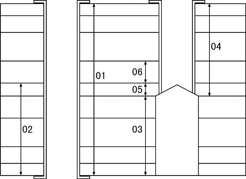
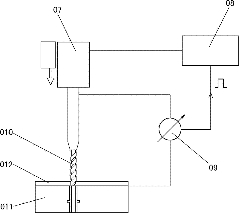
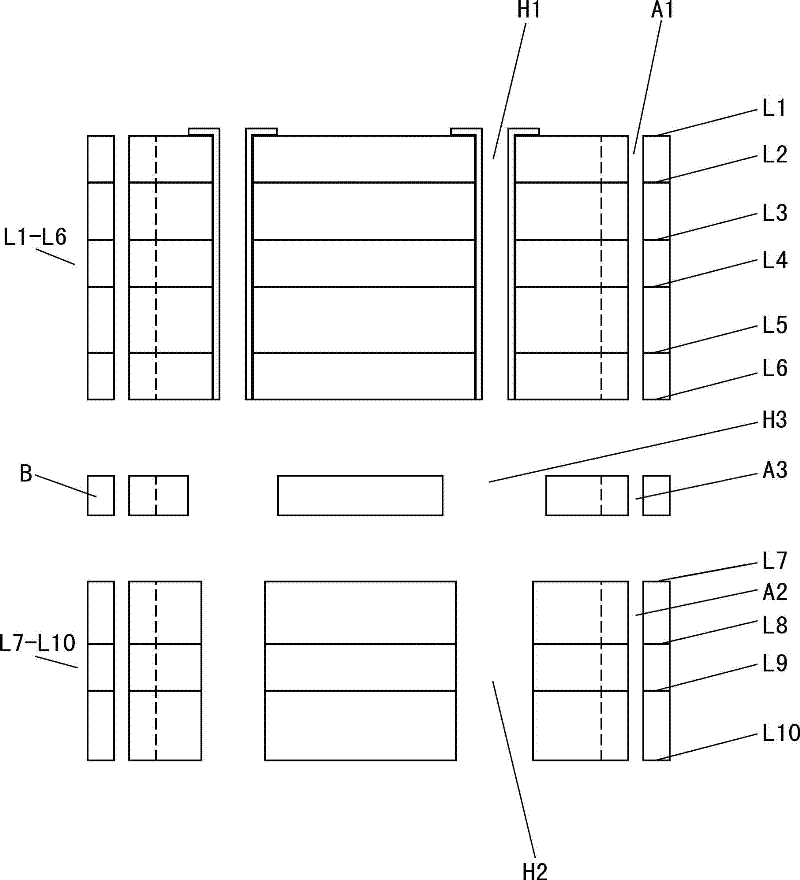
[0030] Such as image 3 , Figure 4 and Figure 5 As shown, the PCB board in this preferred embodiment is a ten-layer board, and the manufacturing method of back-drilling holes on PCB boards with other layers can refer to this preferred embodiment for manufacturing.

[0031] (1) According to the level distribution of metallized holes and non-metallized holes on the PCB board to be produced, the layers L1, L2, L3, L4, L5, L6, L7, L8, L9 of the PCB board will be formed , L10 is divided into each layer L1, L2, L3, L4, L5, L6 that constitutes the metallized hole layer and each layer L7, L8, L9, L10 that constitutes the non-metallized hole layer;

[0032] (2) Each layer L1, L2, L3, L4, L5, and L6 constituting the metallized hole layer is sequentially transferred and pressed to form the metallized hole layer L1-L6, such as image 3 shown; then, a...


PUM


Abstract

The invention discloses a manufacturing method of back drill holes on a PCB (Printed Circuit Board). The manufacturing method comprises the following steps of: in a manufacturing process of the PCB, dividing all layers of the PCB into layers for forming a metalized hole layer and layers for forming a non-metalized hole layer according to layered distribution of metalized holes and non-metalized holes of the back drill holes on the PCB to be manufactured; respectively manufacturing and processing all the layers forming the metalized hole layer and all the layers forming the non-metalized hole layer to form a metalized hole layer with the metalized holes and a non-metalized layer with the non-metalized holes; and laminating the metalized hole layer with the metalized holes and the non-metalized layer with the non-metalized holes through a prepreg with low fluidity to form the PCB with the back drill holes. Therefore, according to the manufacturing method disclosed by the invention, useless hole copper can be completely eliminated, so that the back drill holes without useless hole copper residual can be manufactured on the PCB, and the signal transmission integrity of the PCB is ensured so as to adapt to development requirements of electronic products.

Description

technical field [0001] The invention belongs to the field of PCB board manufacturing, and more specifically, the invention relates to a method for manufacturing back-drilled holes on a PCB board. Background technique [0002] As the transmission rate of electronic products continues to increase, the electronic products have significantly increased requirements on the integrity of the signal transmission of the PCB board (abbreviated as SI). Back-drilling is an important factor in PCB board design, and back-drilling plays the role of electrical connection and fixing devices. [0003] In the production process of PCB board (ie, printed circuit board), the useless hole copper (Stub for short) in the plated through hole (ie, PTH hole) does not work for signal transmission, so the useless hole in the plated through hole needs to be Copper is removed to ensure the integrity of the signal transmission on the PCB. [0004] Such as figure 1 As shown, after the useless hole copper ...

Claims


Application Information

Patent Timeline
Patent Type & Authority Applications(China)
IPC IPC(8): H05K3/42H05K3/46
Inventor 袁欢欣苏维辉杨晓新郑惠芳苏藩春苏启能谢少英杨海永黄函杨润泽李柳坚
Owner CHINA CIRCUIT TECH SHANTOU CORP
Why Eureka
Try Eureka