

Method of electroplating uniform copper layer
A copper layer, deep plating technology, applied in circuits, electrolytic components, electrolytic processes, etc., can solve problems such as high-through hole deep plating ability and low deep plating ability
- Summary
- Abstract
- Description
- Claims
- Application Information
AI Technical Summary
Problems solved by technology
Method used
Image

Examples
Embodiment 1
[0077] By mixing 75g / L copper (copper sulfate pentahydrate), 240g / L sulfuric acid, 50ppm chloride ion, 0.3g / L manganese sulfate aqueous solution, 1mg / L sulfopropyl disulfide, 100ppb sodium 3-mercaptopropanesulfonate Salt and 1.5g / L inhibitor to prepare copper plating solution. The suppressor is an EO / PO copolymer with a molecular weight of less than 5000 and terminal hydroxyl groups. The plating solution includes 5 mg / L of a leveling agent, which is a reaction product of 63 mmol of 1,4 butanediol diglycidyl ether, 25 mmol of imidazole and 75 mmol of 4-phenylimidazole. Analysis of the reaction product showed the following peaks: δppm: 9.22-7.22 (m, 24H, H 芳基 ); 4.52-3.00(m, 37.2H(2.65×14H), 4CH 2 -O, 2CH-OH, 2CH 2 -N); and 1.74-1.24(m, 10.6H(2.653×4H), 2CH 2 ).
Embodiment 2
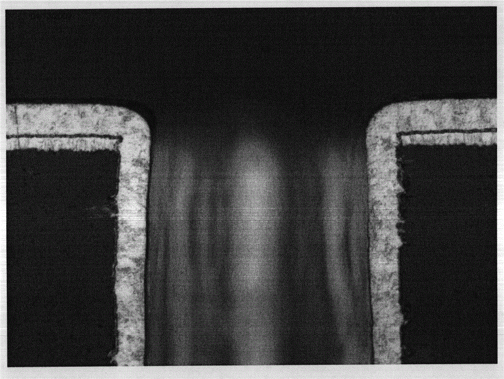
[0079] For double-sided FR4PCB (5×9.5cm) specimens (2.4mm thick) with through-holes with an average diameter of 0.3mm, a thin seed copper layer of 1-3μm is firstly electroless plated by a conventional electroless copper plating solution. Plating was then performed using the copper plating solution of Example 1 in a Haring cell. The temperature of the bath was 25°C. Apply 2A / dm 2 The current density to the sample for 80 minutes. The copper plated coupons were analyzed to determine the inflection point and the throwing power of through holes. Cross-sections were made at multiple places of the sample to visually compare and measure the inflection point and the thickness of the copper plating on the inner wall of the through hole. figure 1 A 5000X SEM with a Leica microscope is one of the through holes. The SEM shows that the thickness of the copper plating is substantially the same on the inner wall of the via and on both sides of the inflection point. The average throwing p...
Embodiment 3
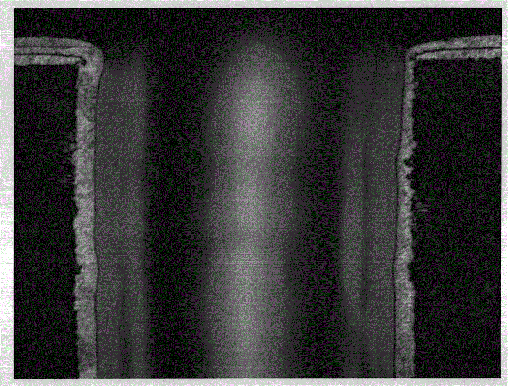
[0081] The method of Example 2 was repeated using the same type of PCB coupon with the same dimensions. The sample described in embodiment 2 carries out electroless copper plating, then carries out electroplating, wherein the copper electroplating solution used is identical with embodiment 1, except not adding 3-mercaptopropanesulfonic acid sodium salt in this copper electroplating solution. Copper electroplating is carried out under the same conditions and electroplating parameters as in Example 2. After the copper plating, the sample is cross-sectioned in multiple places to visually compare and measure the thickness of the copper coating on the surface of the sample and the inner wall of the through hole to determine the inflection point and the deep plating ability of the through hole. The average throwing power of the inflection point was measured to be 55%, and the average throwing power of the through holes was 80%. figure 2 It is a 5000X SEM of one of the through hole...
PUM
 Abstract
Description
Claims
Application Information