Touchable sensing matrix unit of co-constructed active array, active array and display

An active array and touch sensing technology, applied in the field of touch sensing matrix and sensing conduction matrix, can solve the problems of complex manufacturing process, low yield, and difficult to correct pressure sensitivity.

Active Publication Date: 2012-07-04
绿触(香港)国际电子有限公司
View PDF10 Cites 21 Cited by
  • Summary
  • Abstract
  • Description
  • Claims
  • Application Information

AI Technical Summary

Problems solved by technology

[0010] The above two existing touch display panels can indeed integrate the touch panel into a flat-panel display to realize a thinner touch display, but the manufacturing process and structure of the display panel must be changed. Once the display panel manufacturing process and The first challenges faced by the structure are nothing more than the reduction of the yield rate and the increase of the cost of the manufacturing process; Figure 26 In the shown resistive touch display panel, although the upper transparent electrode on the spacer 93 is used as a means of touching the two metal pads to change the voltage value, the spacer 93 must be separated from the TFT array substrate, and the TFT array Each pixel electrode of the substrate must additionally form two metal spacers 971, such as Figure 27 As shown, and additional auxiliary lines for the X-axis and Y-axis not only reduce the visible area of ​​the pixel electrode but also complicate the manufacturing process of the TFT array substrate
[0011] In addition, in the center, periphery and corner of the pixel display area of ​​the glass substrate, because the pressure sensitivity and deformation will be different, the pressure sensitivity is not easy to correct, and it cannot form multi-finger multi-touch sensing, which is also an important technology. defect
[0012] Similarly, the electromagnetic induction touch display panel must also add the first and second direction wires to the color filter substrate manufacturing process structure, so the manufacturing process steps are also changed, the manufacturing process is more complicated, and the number of light rays and costs are greatly increased.

Method used


Image

  • Touchable sensing matrix unit of co-constructed active array, active array and display
  • Touchable sensing matrix unit of co-constructed active array, active array and display
  • Touchable sensing matrix unit of co-constructed active array, active array and display

Examples


example 1

[0117] Example 1: Active Array TFT Liquid Crystal Display (1)

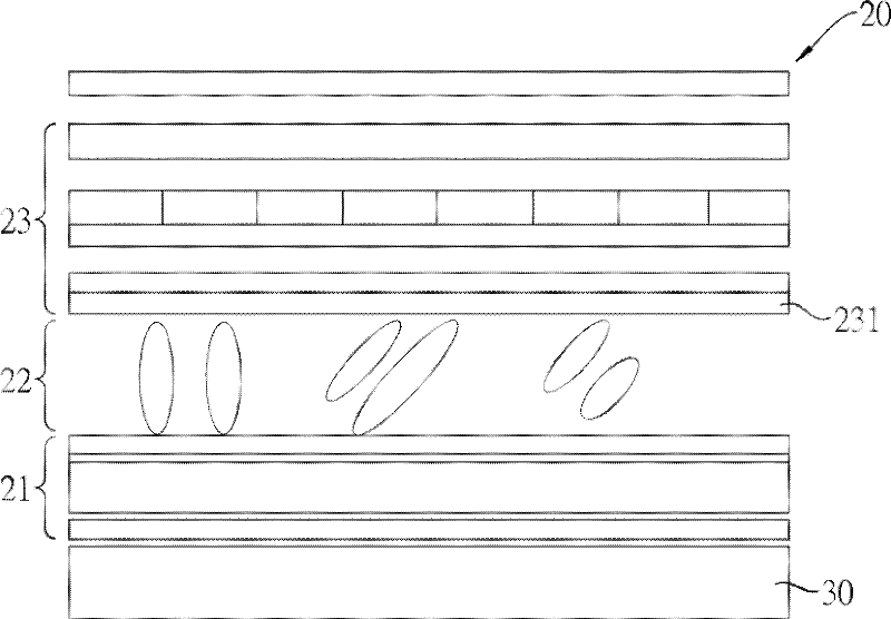
[0118] see figure 2 As shown, in this example, the active matrix TFT liquid crystal display or flat panel display can be a transmissive, reflective, or transflective TFT liquid crystal display or LTPS TFT liquid crystal display, or a microchip on a semiconductor chip. The microdisplay (Liquid Crystal on Silicon, LCoS) formed by the pixel array includes at least one upper substrate 23, which can be a color filter substrate, and the lower active array substrate 21 is a co-configuration touch sensing active array, with The liquid crystal layer 22 ; and the common electrode 231 is formed on the upper color filter substrate 23 . If it is a transmissive display, at least one backlight module 30 is further included under the display. Considering the shielding of the signal of the common electrode 231 to the signal of the capacitive touch sensing, the application of this example to the electromagnetic induction touch i...

example 2

[0119] Example 2: Active Array TFT Liquid Crystal Display (2)

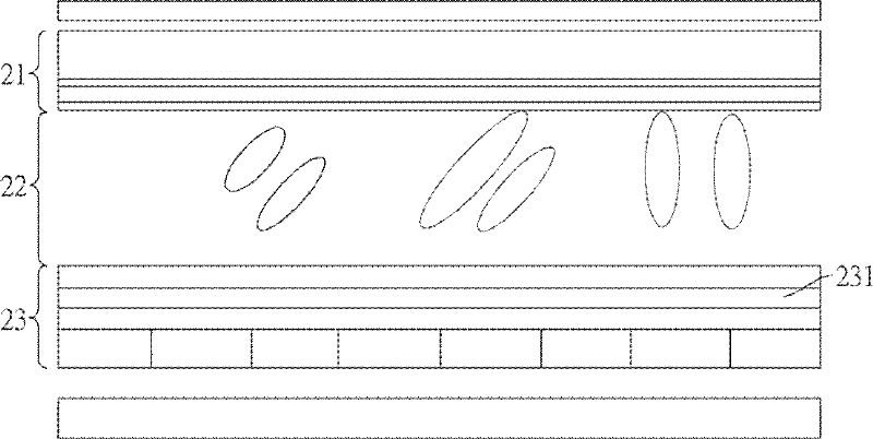
[0120] In this example, as image 3 As shown, the active array TFT liquid crystal display or flat panel display can be a transmissive TFT liquid crystal display or LTPS TFT liquid crystal display, which includes at least one upper active array substrate 21 which is a co-configured touch sensing active array and a lower color filter The substrate 23 interposes the liquid crystal layer 22 therebetween; and the first and second sensing conductive lines of the touch sensing matrix of the present invention are the data lines and scanning lines on the active array of the upper active array substrate 21 . According to the design of the co-configured touch sensing active array element, the multiple first sensing conductive lines and / or multiple second sensing conductive lines of the touch sensing matrix may be signal lines, reading lines, or bias lines, Or the control line, or part of the pixel circuit, or part of the au...

example 3

[0122] Example 3: The active matrix TFT display or flat panel display in this example is roughly the same as in Example 1, see Figure 5 As shown, it is a fringe field switching wide viewing angle (Fringe Field Switching Wide Viewing Angle) TFT liquid crystal display, which at least includes a lower active array substrate 21, an upper substrate 23' and a polarizer 24, and a liquid crystal molecule is interposed therebetween Layer 22 (LC molecule layer) is a negative type liquid crystal (ΔN=Ne-No<0) arranged horizontally; wherein the lower active array substrate 21 includes a first substrate 211, a pixel electrode layer 212 (pixel layer), a common Electrode layer 213 (common electrode layer).

[0123] The above-mentioned common electrode layer 213 and pixel electrode layer 212 are both arranged on the same side of the first substrate 211, and its structure is designed such that the fringe electric field is Figure 6 As shown in the common electrode layer 213 of the upper subst...


PUM


Abstract

The present invention relates to a touchable sensing matrix unit, a co-constructed active array substrate having the touchable sensing matrix unit and a display having the co-constructed active array substrate. The touchable sensing matrix unit is formed on the co-constructed active array substrate and has multiple first sensing and transmitting wires and multiple second sensing and transmitting wires. The first and second sensing and transmitting wires are conductive and cyclic, intersect to form an angle, and sandwich an insulation layer formed therebetween. The touchable sensing matrix unit has at least one set of wires of the co-constructed active array substrate and an improved design using the at least one set of wires.

Description

technical field [0001] The present invention relates to an active array display integrating touch functions, in particular to a touch sensing matrix arranged on a common configuration active array, the wire wiring of the touch sensing matrix includes a plurality of first sensing conductive lines and a plurality of A second induction conduction line is interlaced with each other to form an induction conduction matrix with a certain angle, conductivity and certain periodicity. Background technique [0002] Due to the sophistication of touch panels, the yield rate of touch panels has increased and the touch accuracy has become more accurate. Touch panels can be divided into electromagnetic, resistive, capacitive, and optical (infrared, ultrasonic, etc.) based on the principle of touch sensing. )etc. [0003] In order to provide user input functions for thin, light and miniaturized electronic products, it is a feasible space-saving method to superimpose a touch panel on the scr...

Claims


Application Information

Patent Timeline
Patent Type & Authority Applications(China)
IPC IPC(8): G06F3/041
CPCG06F3/042G06F3/046G06F3/0416G06F2203/04106G06F3/044G06F3/0412G06F3/04166G06F3/0445G06F3/0446
Inventor 刘鸿达
Owner 绿触(香港)国际电子有限公司
Why Eureka
Try Eureka