Cell layout for multiple patterning technology

A pattern and sub-pattern technology, applied in the field of cell layout of multiple patterning technology, can solve the problems of area loss, invalid timing optimization, low utilization rate, etc.

Active Publication Date: 2012-07-04
TAIWAN SEMICON MFG CO LTD
View PDF4 Cites 12 Cited by
  • Summary
  • Abstract
  • Description
  • Claims
  • Application Information

AI Technical Summary

Problems solved by technology

Inserting large buffers within standard cell boundaries can lead to area penalties, while imposing complex cell adjacency constraint

Method used


Image

  • Cell layout for multiple patterning technology
  • Cell layout for multiple patterning technology
  • Cell layout for multiple patterning technology

Examples


Embodiment Construction

[0031] The making and using of various embodiments of the invention are discussed in detail below. It should be appreciated, however, that the present invention provides many applicable concepts that can be implemented in a wide variety of specific contexts. The specific embodiments discussed are merely illustrative of specific ways to make and use the invention, and do not limit the scope of the invention.

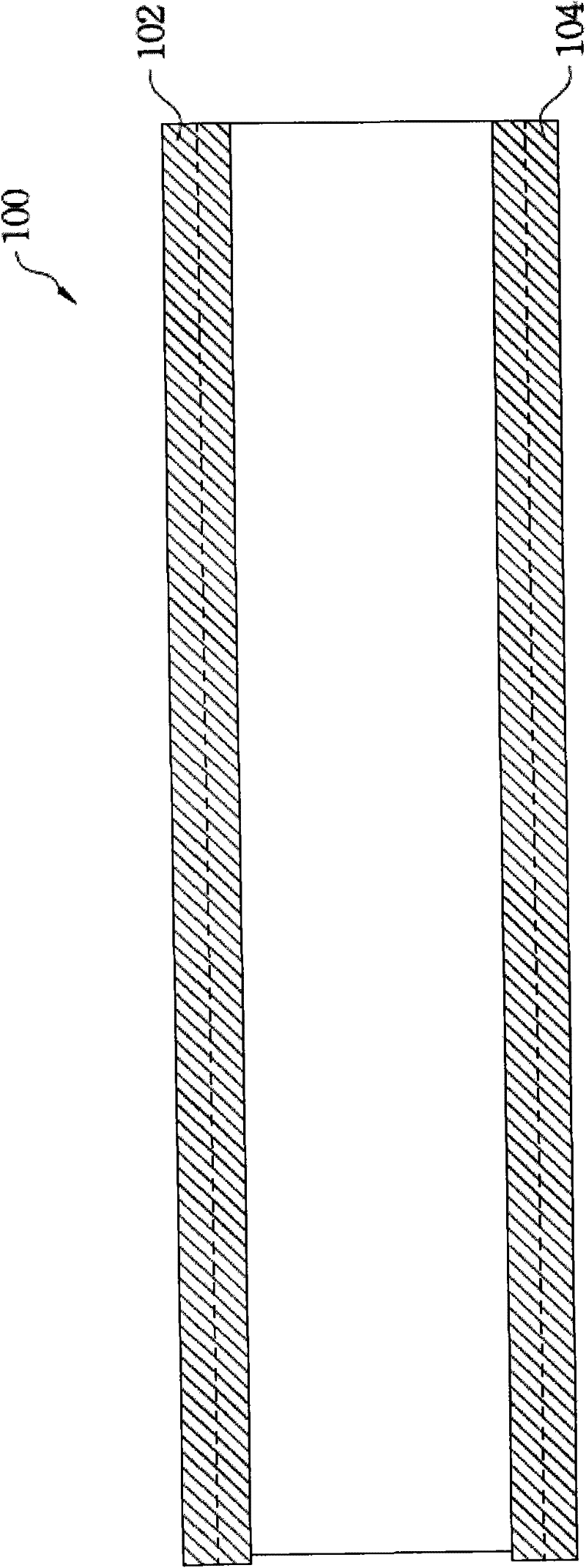
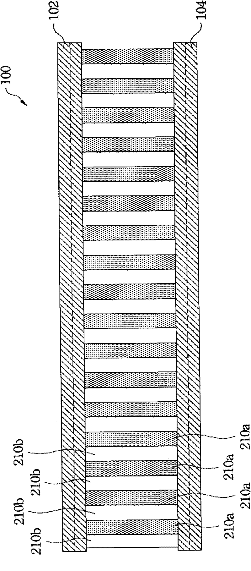
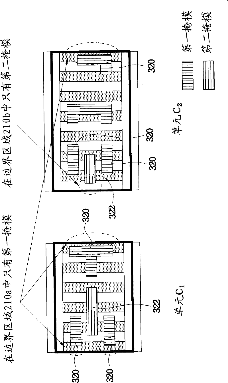
[0032] Figure 1-Figure 4 A process of a cell arrangement according to an embodiment is shown. first reference figure 1 , shows a layout area 100 in which cells are laid out. This unit (referenced below Figure 2-Figure 4 described) may represent any functional block of circuitry, wires, vias, etc. that need to be patterned, and may be on a substrate (eg, polysilicon layer) or on a metallization layer. For example, the cell may represent circuitry and / or wiring associated with memory cells, sense amplifiers, power supply circuits, and the like. It should be noted th...


PUM


Abstract

A system and method for providing a cell layout for multiple patterning technology is provided. An area to be patterned is divided into alternating sites corresponding to the various masks. During a layout process, sites located along a boundary of a cell are limited to having patterns in the mask associated with the boundary site. When placed, the individual cells are arranged such that the adjoining cells alternate the sites allocated to the various masks. In this manner, the designer knows when designing each individual cell that the mask pattern for one cell will be too close to the mask pattern for an adjoining cell.

Description

technical field [0001] The present invention relates to the field of integrated circuits, and more particularly, to cell layouts for multiple patterning techniques. Background technique [0002] In lithography systems, in order to obtain good, high-density, high-resolution patterns, high resolution is required. In photolithography systems employed in the integrated circuit (IC) industry, light is projected onto a photoresist in order to pattern electronic devices. The dramatic change in the resolution of lithography systems is one of the most important driving factors for the manufacture of high-density and high-speed semiconductor IC chips. [0003] In general, the resolution of a lithography system depends, among other things, on the wavelength of the light. Wavelengths decrease gradually from the mercury G-line (436nm) to the ArF excimer laser line (193nm), and further down to 157nm, and possibly into extreme ultraviolet radiation (EUV) wavelengths. Other techniques su...

Claims


Application Information

Patent Timeline
IPC IPC(8): G06F17/50
CPCG06F17/50G03F7/70433G03F1/70G03F7/70466G03F7/2022H01L21/0275
Inventor 陈皇宇侯元德谢艮轩刘如淦鲁立忠
Owner TAIWAN SEMICON MFG CO LTD
Why Eureka
Try Eureka