Method for embedding multiple conductive terminals in circuit board, and conductive terminal

A technology of conductive terminals and circuit boards, applied in circuits, electrical components, circuit/collector parts, etc., can solve the problems of easy deformation of conductive terminals, many operation steps, and inability to meet the requirements of light and thin products.

Active Publication Date: 2012-07-04
DEYI PRECISION ELECTRONIC IND CO LTD PANYU
View PDF3 Cites 2 Cited by
  • Summary
  • Abstract
  • Description
  • Claims
  • Application Information

AI Technical Summary

Problems solved by technology

[0002] At present, there are mainly two ways of connecting electronic components and circuit boards in the prior art: one is to conduct electrical connection through an electrical connector, and the electrical connector mainly includes an insulating body and a plurality of conductive terminals accommodated in the insulating body , and the insulating body stays on the circuit board as the conductive terminals are soldered to the circuit board. There are many components, which makes the overall structure complex, and it is necessary to set a holding structure on the conductive terminals to fix them in the insulating body, which cannot meet the light and thin requirements of the product. Requirements, this kind of structure makes the operation steps from making the electrical connector to welding on the circuit board relatively many and complicated; the other is to directly plant the conductive terminals on the circuit board without the insulating body, although it meets the requirements of light and thin products. , but before the conductive terminal is soldered to the circuit board, when the manufacturer goes to the client to carry out the welding operation, the vulnerable part of the conductive terminal is more likely to be deformed or damaged during transportation, resulting in quality problems in the later stage

Method used


Image

  • Method for embedding multiple conductive terminals in circuit board, and conductive terminal
  • Method for embedding multiple conductive terminals in circuit board, and conductive terminal
  • Method for embedding multiple conductive terminals in circuit board, and conductive terminal

Examples


specific Embodiment approach

[0036] The present invention will be further described below in conjunction with accompanying drawing and specific embodiment:

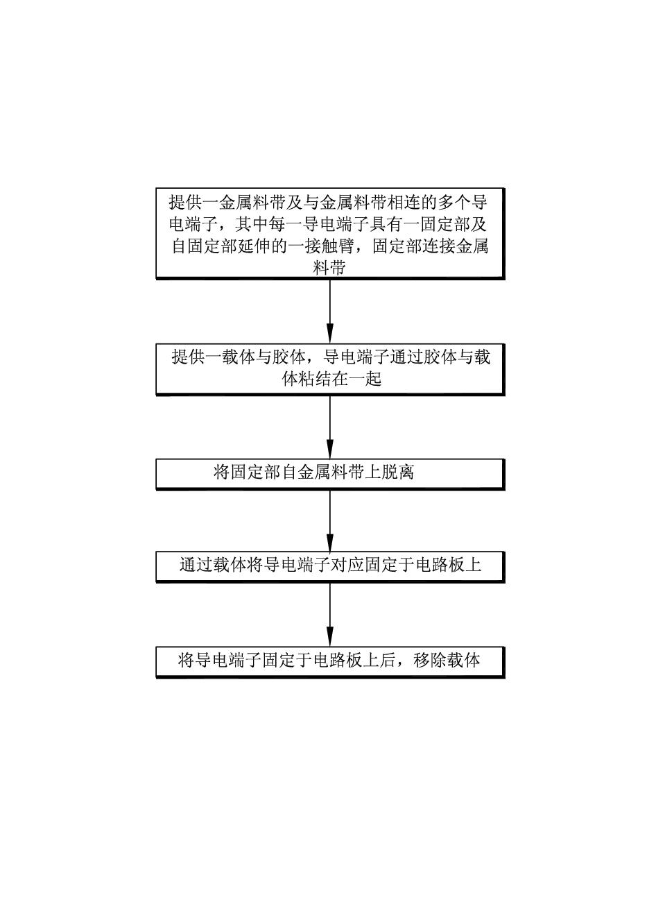
[0037] Please refer to figure 1 A schematic flow chart of the implementation of the present invention, a method for planting a plurality of conductive terminals on a circuit board includes the following steps.

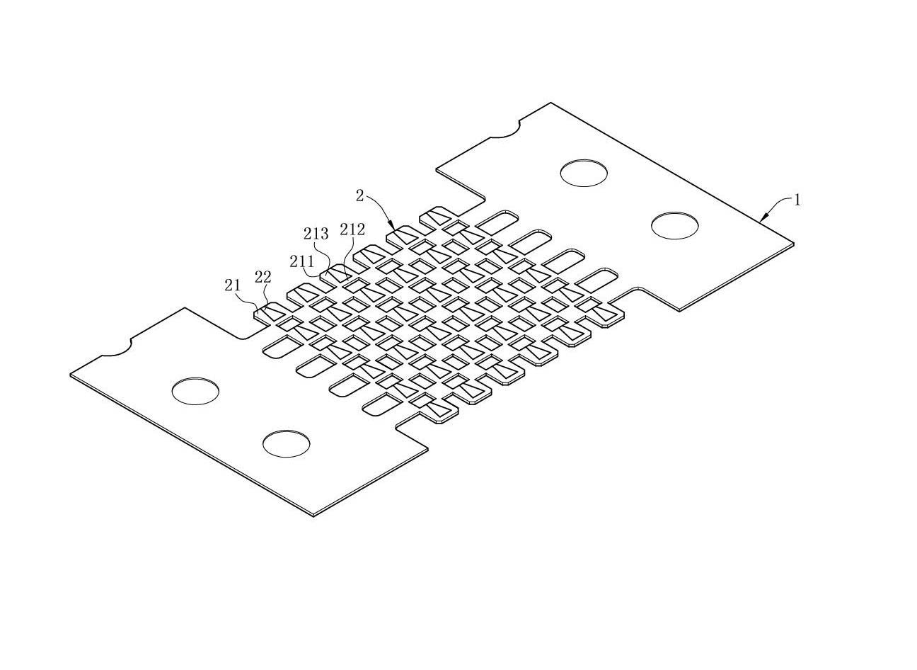
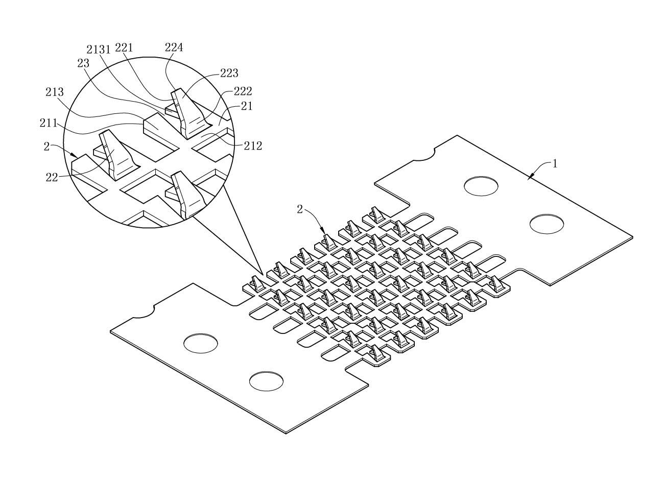
[0038] Please refer to image 3 , Step 1: providing a metal strip 1 and a plurality of conductive terminals 2 connected to the metal strip 1 .

[0039] A plurality of the conductive terminals 2 are arranged in a matrix, each of the conductive terminals 2 has a fixing portion 21 and a contact arm 22 extending from the fixing portion 21 .

[0040] The fixing portion 21 is flat and roughly rectangular, and each adjacent two sides form a chamfered side 211 (such as Figure 6 ), the fixing portion 21 is connected to the metal strip 1 at the chamfered edge 211. The fixing part 21 has a first plate 212 and two second plates ...


PUM


Abstract

The invention provides a method for embedding multiple conductive terminals in a circuit board. The method comprises the following steps of: supplying a metal material band and the multiple conductive terminals connected with the metal material band, wherein each conductive terminal is provided with a fixing part and a contact arm extending from the fixing part; and the fixing parts are connected with the metal material band; supplying a carrier and a colloid, wherein the conductive terminals are adhered with the carrier through the colloid; separating the fixing parts from the metal material band; correspondingly fixing the conductive terminals on the circuit board through the carrier; and after the conductive terminals are fixed on the circuit board, removing the carrier. The colloid is used for adhering the conductive terminals and the carrier, so that the conductive terminals are convenient to transport before the conductive terminals are fixed on the circuit board and difficult to fall down during transportation; furthermore, elements, such as an insulation body, are not needed; and therefore, a structure for electrically connecting an electronic element and the circuit board is simplified, and the method is operated easily, conveniently and quickly.

Description

technical field [0001] The invention relates to a method for planting a plurality of conductive terminals on a circuit board and the conductive terminal. Background technique [0002] At present, there are mainly two ways of connecting electronic components and circuit boards in the prior art: one is to conduct electrical connection through an electrical connector, and the electrical connector mainly includes an insulating body and a plurality of conductive terminals accommodated in the insulating body , and the insulating body stays on the circuit board as the conductive terminals are soldered to the circuit board. There are many components, which makes the overall structure complex, and it is necessary to set a holding structure on the conductive terminals to fix them in the insulating body, which cannot meet the light and thin requirements of the product. Requirements, this kind of structure makes the operation steps from making the electrical connector to welding on the ...

Claims


Application Information

Patent Timeline
Patent Type & Authority Applications(China)
IPC IPC(8): H01R12/55H01R43/00H01R43/02
Inventor 龚永生林三祐
Owner DEYI PRECISION ELECTRONIC IND CO LTD PANYU
Why Eureka
Try Eureka