Hexamethylene diisocyanate (HDI) plate with symmetrically pressed structure and manufacturing method thereof

A production method and symmetrical technology, which is applied in multilayer circuit manufacturing, electrical components, printed circuit components, etc., can solve problems such as difficult control of the expansion and contraction of the broken plate, asymmetrical lamination structure, and deviation of the secondary lamination layer. Achieve the effects of easy control of expansion and contraction, improvement of layer deviation, and reduction of production difficulty

Inactive Publication Date: 2012-07-04
SHENZHEN SUNTAK MULTILAYER PCB
View PDF2 Cites 25 Cited by
  • Summary
  • Abstract
  • Description
  • Claims
  • Application Information

AI Technical Summary

Problems solved by technology

[0006] For this reason, the object of the present invention is to provide a kind of HDI plate of symmetrical lamination structure and its manufacturing method, to solve the problems of asymmetry of lamination structure in the production of existing HDI boards, which may easily lead to wear out, breakage of the plate, and expansion and contraction of the plate. It is difficult to control, and it is easy to cause the problem of layer deviation in the second pressing

Method used


Image

  • Hexamethylene diisocyanate (HDI) plate with symmetrically pressed structure and manufacturing method thereof
  • Hexamethylene diisocyanate (HDI) plate with symmetrically pressed structure and manufacturing method thereof
  • Hexamethylene diisocyanate (HDI) plate with symmetrically pressed structure and manufacturing method thereof

Examples


Embodiment Construction

[0035] In order to illustrate the idea and purpose of the present invention, the present invention will be further described below in conjunction with the accompanying drawings and specific embodiments.

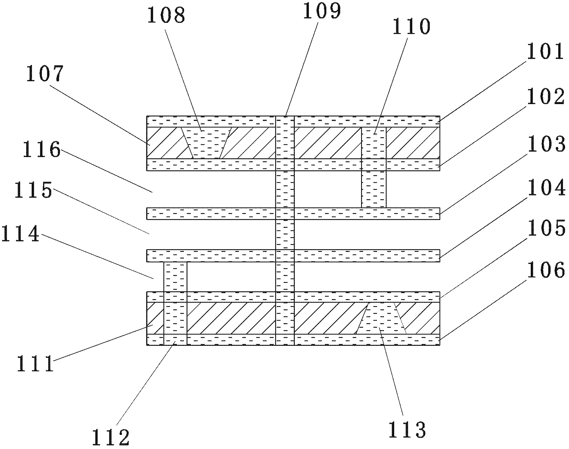
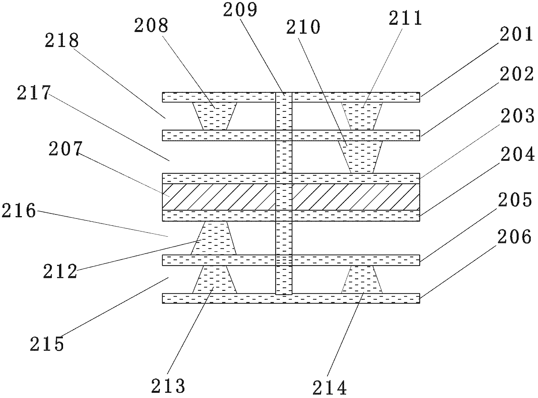
[0036] See figure 2 as shown, figure 2 It is a schematic diagram of the HDI plate structure of the six-layer laser drilling of the present invention. The present invention provides a HDI board with a symmetrical laminated structure. The HDI board specifically includes a core board 207, and the upper and lower sides of the core board 207 are provided with a third copper foil layer 203 and a fourth copper foil layer 204. The third Circuit patterns are formed on the copper foil layer 203 and the fourth copper foil layer 204 .

[0037] A third prepreg 217 is pasted on the third copper foil layer 203, a second copper foil layer 202 is pasted on the third prepreg 217, a fourth prepreg 218 is pasted on the second copper foil layer 202, and a fourth prepreg 218 is pasted on the t...


PUM


Abstract

The invention discloses a hexamethylene diisocyanate (HDI) plate with a symmetrically pressed structure and a manufacturing method thereof. The manufacturing method comprises the following steps of: A, pressing a second copper foil layer on the upper side of a core plate, and pressing a fifth copper foil layer on the lower side of the core plate; B, performing laser hole drilling on the second copper foil layer to form a second laser blind hole, and performing laser hole drilling on the fifth copper foil layer to form a fourth laser blind hole; C, pressing a first copper foil layer on the second copper foil layer, and pressing a sixth copper foil layer on the fifth copper foil layer; and D, performing laser hole drilling on the first copper foil layer to form a first laser blind hole and a third laser blind hole, performing laser hole drilling on the sixth copper foil layer to form a fifth laser blind hole and a sixth laser blind hole, wherein the third laser blind hole is stacked with the second laser blind hole, and the fifth laser blind hole is stacked with the fourth laser blind hole. Compared with the prior art, the HDI plate has the advantages that the pressed stacked structure is changed; asymmetric pressing is replaced by symmetric pressing; after pressing for the first time, one core plate replaces two core plates; the expansion and contraction of the HDI plate are easy to control during manufacturing; and furthermore, layer deflection is improved greatly, the manufacturing difficulty is reduced greatly, and the production period is shortened.

Description

Technical field: [0001] The invention belongs to the technical field of circuit board production, and in particular relates to a symmetrical lamination structure HDI board and a production method. Background technique: [0002] HDI circuit board, also known as high-density interconnection board, is a circuit board with relatively high circuit distribution density using micro-blind buried hole technology, which can reduce the production cost of multi-layer PCB boards, increase circuit density, high reliability, and power Good performance and other advantages. [0003] At present, the production process of HDI circuit board is as follows: figure 1 As shown, taking a six-layer laser-drilled HDI board as an example, copper foil layers 101 and 102 are arranged on the upper and lower sides of the core board 107, and copper foil layers 105 and 106 are arranged on the upper and lower sides of the core board 111. 105 to make an inner layer circuit pattern, and perform inner layer e...

Claims


Application Information

Patent Timeline
Patent Type & Authority Applications(China)
IPC IPC(8): H05K1/00H05K1/02H05K3/46
Inventor 黄海蛟彭卫红杜明星林楠白亚旭
Owner SHENZHEN SUNTAK MULTILAYER PCB
Why Eureka
Try Eureka