Driving method for liquid crystal panel, display driving circuit and liquid crystal display device

A liquid crystal panel and display driving technology, which is applied to display driving circuits, liquid crystal display devices, and the driving field of liquid crystal panels, can solve the problems of large difference in uniformity between the center and surrounding areas, intensified variation, poor image quality, etc., and achieves display brightness. The effect of uniformity, improved taste, and improved charging time difference

Inactive Publication Date: 2012-07-11
TCL CHINA STAR OPTOELECTRONICS TECH CO LTD
View PDF3 Cites 49 Cited by
  • Summary
  • Abstract
  • Description
  • Claims
  • Application Information

AI Technical Summary

Problems solved by technology

[0002] At present, the resolution and size of liquid crystal displays are getting larger and larger. figure 1 As shown, the equivalent resistance and capacitive load on the equivalent transmission path corresponding to the panel with the thin film transistor (TFT) as the main driving method is getting larger and larger, as shown in figure 2 As shown, this will cause the data signal output by the data driver circuit (Data IC) and the gate control signal output by the gate driver circuit (gate IC) to vary, which is usually called the resistance-capacitance delay effect (RC delay) in the industry, such as image 3 As shown, when the resolution and size increase, the resistance-capacitance delay effect (RC delay) becomes larger and the variation intensifies. Take the bilateral gate drive circuit (gate IC) and the single-side data drive circuit (Data IC) drive as examples. The middle The variation of the gate control signal is the most serious, and the variation of the data signal at the lower end is the most serious. In this way, the uniformity of the center and the periphery is quite different, and the image quality seen is poor.

Method used


Image

  • Driving method for liquid crystal panel, display driving circuit and liquid crystal display device
  • Driving method for liquid crystal panel, display driving circuit and liquid crystal display device
  • Driving method for liquid crystal panel, display driving circuit and liquid crystal display device

Examples


Embodiment Construction

[0028] The present invention will be further described below in conjunction with the accompanying drawings and preferred embodiments.

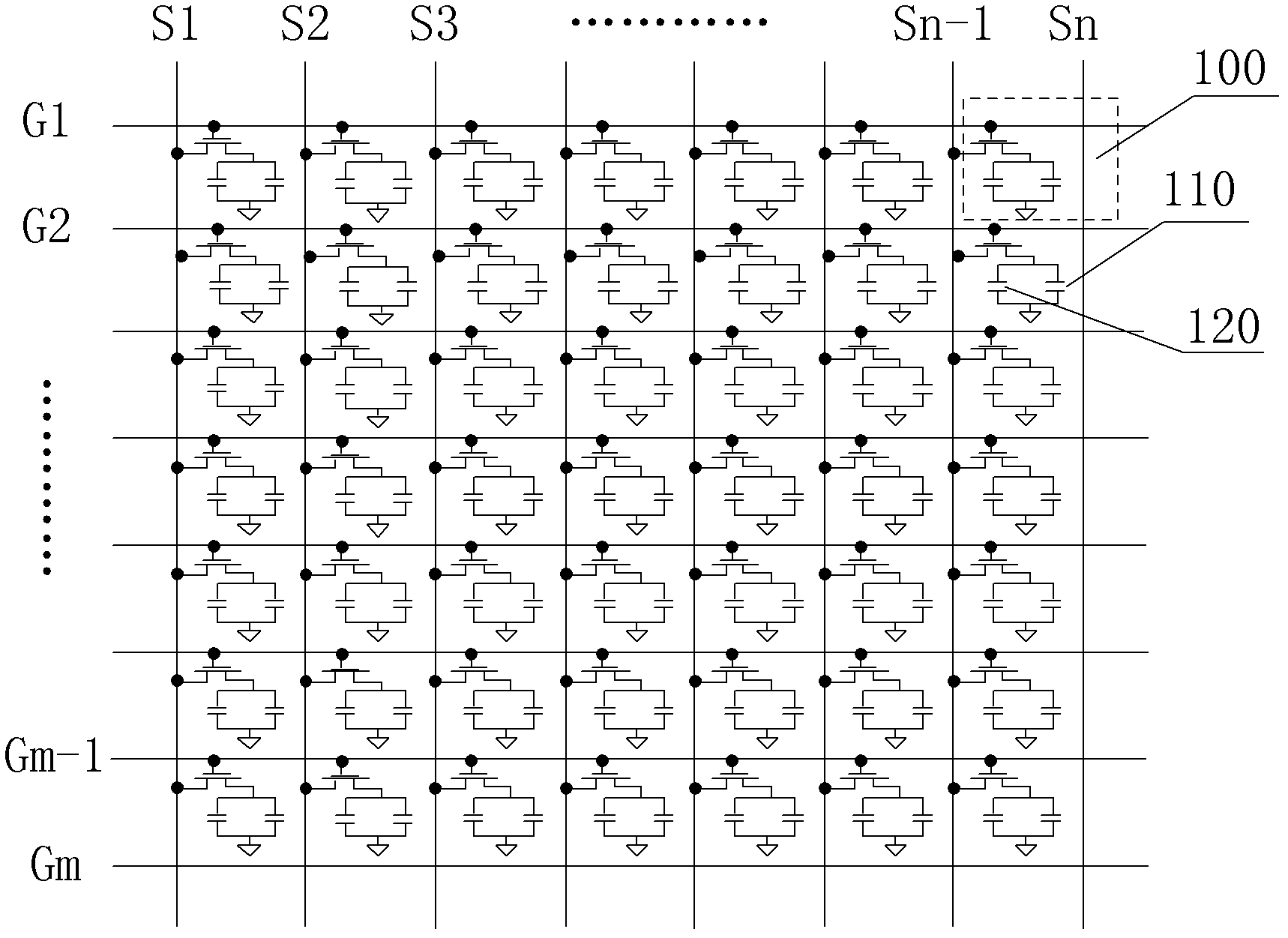
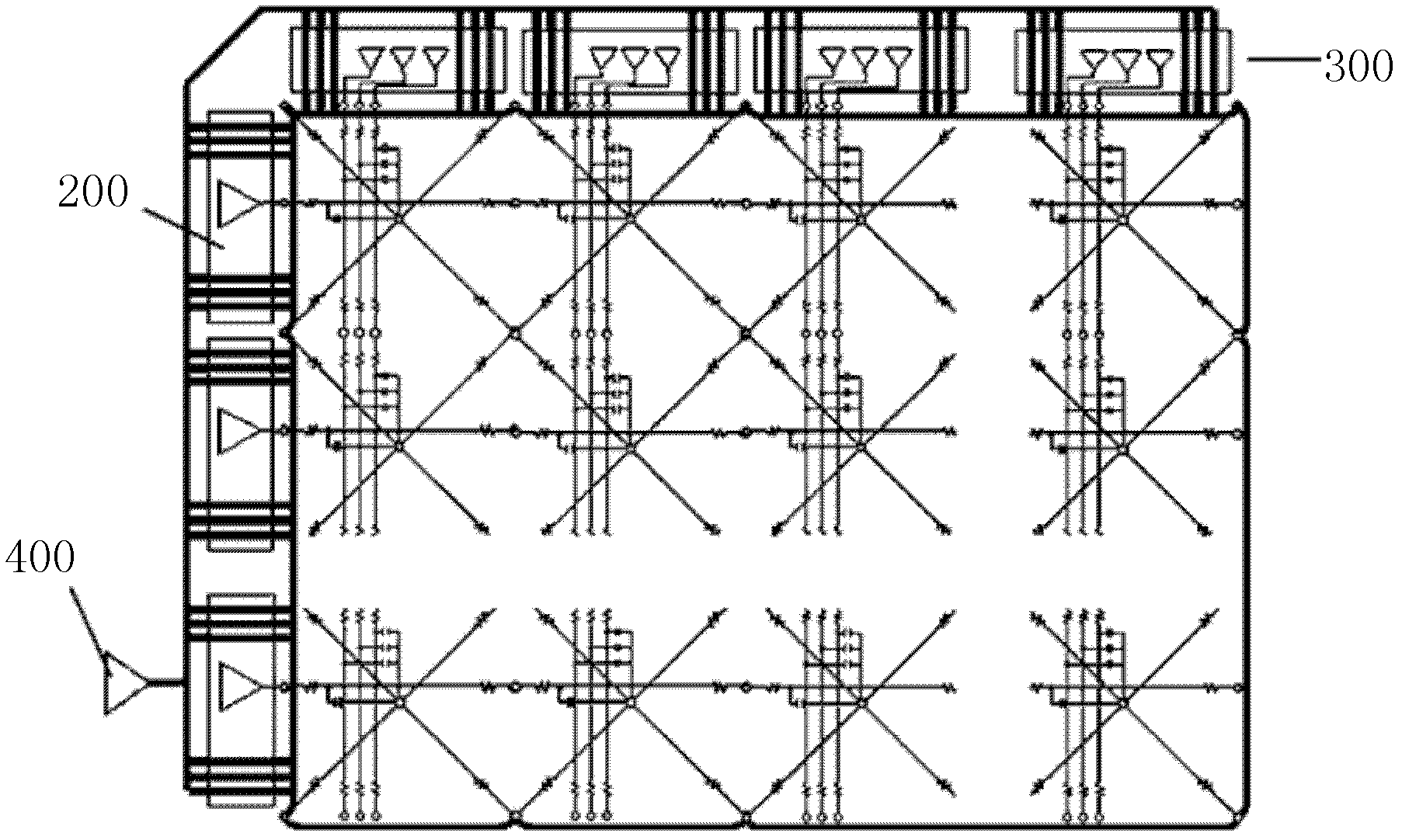
[0029] A liquid crystal display device includes a liquid crystal panel. like figure 1 As shown, the liquid crystal panel includes criss-cross scanning lines and data lines, G1 ~ Gm-1 are scanning lines, S1 ~ Sn are data lines, and the matrix formed by scanning lines and data lines is a thin film transistor 100 (TFT). The source is connected to the data line, the gate of the TFT is connected to the scan line, and a liquid crystal capacitor 110 and a storage capacitor 120 arranged in parallel are connected between the drain of the TFT and the common electrode. The liquid crystal panel of the present invention includes a display driving circuit, including scanning lines, data lines, a gate driving circuit 200 connected to the scanning lines, and a data driving circuit 300 connected to the data lines. Determine the voltage compensation module fo...


PUM


Abstract

The invention discloses a driving method for a liquid crystal panel, a display driving circuit and a liquid crystal display device. The driving method for the liquid crystal panel comprises the following steps: A, acquiring a coordinate position of a pixel to be displayed of a current frame of the liquid crystal panel and an ideal voltage value required by a gray level for corresponding displaying the pixel; and B, according to the coordinate position of the current pixel on the liquid crystal panel, determining an offset voltage for promoting the uniformity of the liquid crystal panel and then loading the offset voltage onto a corresponding data line. According to the invention, the difference of charging time in each region, which is generated due to charging caused by resistance-capacitance waveform delay variation (resistance-capacitance delay (RC delay)), of the liquid crystal panel is effectively improved; the display uniformity of the liquid crystal panel, particularly a large-scale liquid crystal panel, is promoted; and the taste performance of the liquid crystal panel is improved.

Description

technical field [0001] The invention relates to the field of liquid crystal display, and more specifically, relates to a driving method of a liquid crystal panel, a display driving circuit and a liquid crystal display device. Background technique [0002] At present, the resolution and size of liquid crystal displays are getting larger and larger. figure 1 As shown, the equivalent resistance and capacitive load on the equivalent transmission path corresponding to the panel with the thin film transistor (TFT) as the main driving method is getting larger and larger, as shown in figure 2 As shown, this will cause the data signal output by the data driver circuit (Data IC) and the gate control signal output by the gate driver circuit (gate IC) to vary, which is usually called the resistance-capacitance delay effect (RC delay) in the industry, such as image 3 As shown, when the resolution and size increase, the resistance-capacitance delay effect (RC delay) becomes larger and ...

Claims


Application Information

Patent Timeline
Patent Type & Authority Applications(China)
IPC IPC(8): G09G3/36G09G3/34G02F1/133G02F1/1362
CPCG02F1/1362G02F1/133G09G2320/0223G02F1/13454G09G3/3611G09G3/34G09G3/36
Inventor 林柏伸谭小平
Owner TCL CHINA STAR OPTOELECTRONICS TECH CO LTD
Why Eureka
Try Eureka