Manufacturing method of multilayer circuit board and laminated structure for multilayer circuit board

A technology of a multilayer circuit board and a manufacturing method, which is applied in the direction of manufacturing a multilayer circuit, etc., can solve the problems of high manufacturing cost, poor thickness uniformity of the insulating layer, lamination depression of the insulating layer, etc., so as to reduce the manufacturing cost and reduce the number of grindings. , the effect of improving uniformity

Active Publication Date: 2012-07-11
新方正控股发展有限责任公司
View PDF3 Cites 5 Cited by
  • Summary
  • Abstract
  • Description
  • Claims
  • Application Information

AI Technical Summary

Problems solved by technology

[0004] In the lamination method in the prior art, on the one hand, if the thickness of the prepreg is small, the uniformity of the thickness of the insulating layer is poor, and defects such as lamination depressions and white spots are prone to appear on the surface of the insulating layer.
On the other hand, because the thickness of the prepregs to be stacked needs to ensure that the insulating layer is fully filled and no voids will occur, the thickness of the prepregs to be stacked is relatively thick. Generally speaking, the thi

Method used


Image

  • Manufacturing method of multilayer circuit board and laminated structure for multilayer circuit board
  • Manufacturing method of multilayer circuit board and laminated structure for multilayer circuit board
  • Manufacturing method of multilayer circuit board and laminated structure for multilayer circuit board

Examples


Embodiment Construction

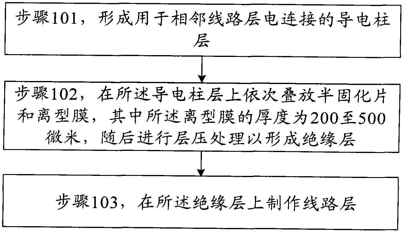
[0021] The present invention provides a kind of manufacturing method of multilayer circuit board, it is characterized in that, comprises the following steps:

[0022] forming a conductive column layer for electrical connection of adjacent circuit layers;

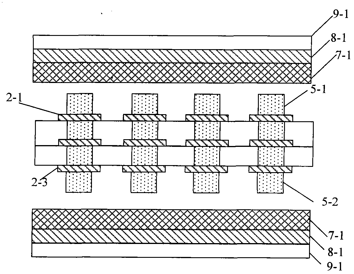
[0023] Laying a prepreg and a release film sequentially on the conductive post layer, wherein the release film has a thickness of 200 to 500 microns, followed by lamination to form an insulating layer;

[0024] A circuit layer is fabricated on the insulating layer.

[0025] Preferably, in each embodiment of the present invention,

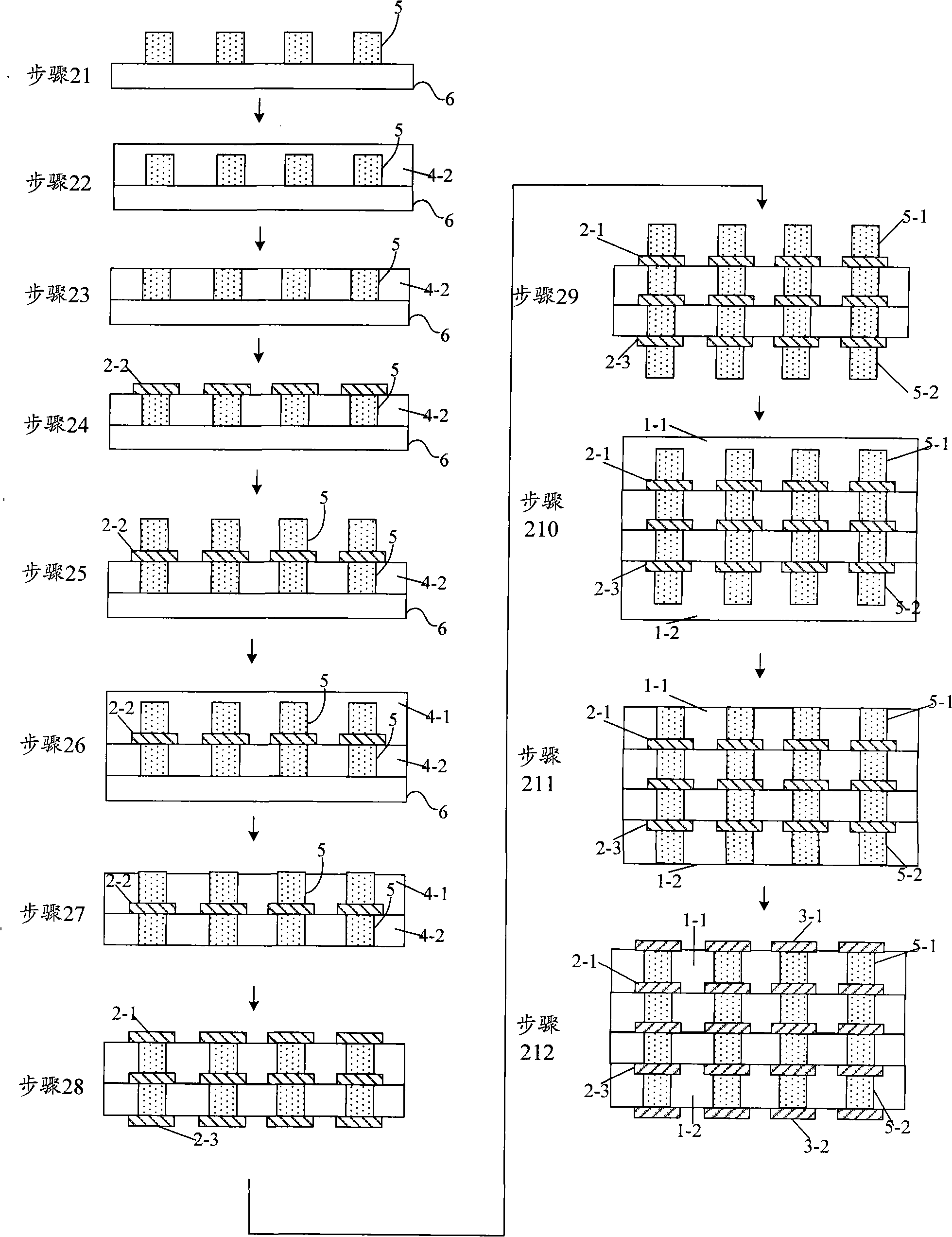
[0026] The forming of the conductive column layer for electrical connection of adjacent circuit layers includes: forming a first conductive column layer and a second conductive column layer;

[0027] The step of sequentially stacking a prepreg and a release film on the conductive column layer, followed by lamination to form an insulating layer includes: sequentially stacking a prepreg and a rele...


PUM

PropertyMeasurementUnit
Thicknessaaaaaaaaaa
Thicknessaaaaaaaaaa

Abstract

The embodiment of the invention discloses a manufacturing method of a multilayer circuit board and a laminated structure for the multilayer circuit board, relating to the field of circuit board manufacturing, and being capable of effectively improving the uniformity of the thickness of an insulating layer. The manufacturing method of the multilayer circuit board comprises the following steps of: forming a conductive column layer for electrically connecting adjacent circuit layers; stacking a prepreg and a release film on the conductive column layer in turn, and laminating to form the insulating layer, wherein the thickness of the release film is 200 to 500 microns; and manufacturing a circuit layer on the insulating layer. The manufacturing method can be used for manufacturing the multilayer circuit board.

Description

technical field [0001] The invention relates to the field of circuit board manufacturing, in particular to a method for manufacturing a multilayer circuit board. Background technique [0002] Multi-layer circuit board is the product of the development of electronic technology in the direction of high speed, multi-function, large capacity and small volume. As the name implies, a multi-layer circuit board includes multiple layers of circuit layers superimposed on each other, an insulating layer is provided between two adjacent circuit layers, and the connection between the circuit layers of each layer is realized through the via holes or conductive pillars passing through the insulating layer. electrical connection. [0003] In the production process of high-performance packaged multilayer circuit boards, conductive pillars (usually copper pillars) are generally used to realize the electrical connection between the circuit layers of each layer, and the purpose of increasing t...

Claims


Application Information

Patent Timeline
IPC IPC(8): H05K3/46
Inventor 朱兴华苏新虹
Owner 新方正控股发展有限责任公司
Why Eureka
Try Eureka