Wide dynamic range time delay integration CMOS image sensor

A technology of time-delay integration and wide dynamic range, which is applied in the direction of image communication, TV, color TV parts, etc., can solve the problem of limiting the dynamic range of sensors and achieve simple results

Inactive Publication Date: 2012-07-18
TIANJIN UNIV
View PDF2 Cites 14 Cited by
  • Summary
  • Abstract
  • Description
  • Claims
  • Application Information

AI Technical Summary

Problems solved by technology

However, the output signal at this time will reach satu...

Method used


Image

  • Wide dynamic range time delay integration CMOS image sensor
  • Wide dynamic range time delay integration CMOS image sensor
  • Wide dynamic range time delay integration CMOS image sensor

Examples


Embodiment Construction

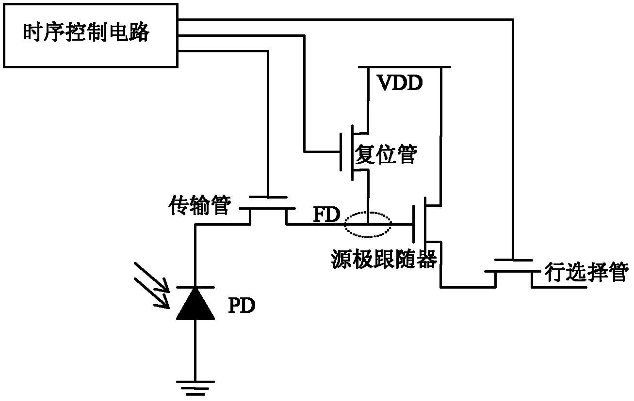
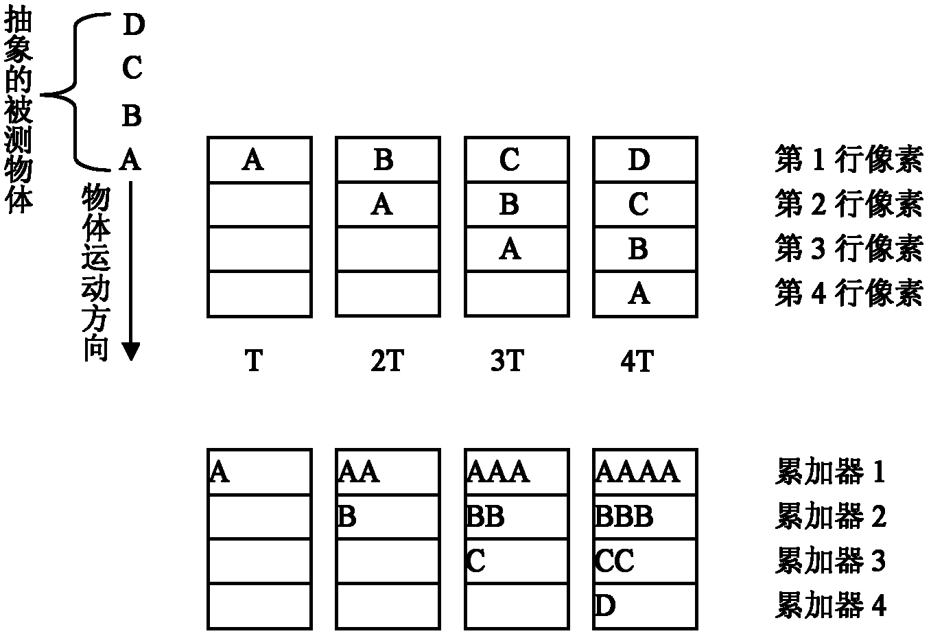
[0036] The CMOS image sensor involved in the present invention works in TDI mode, which requires relative movement between the sensor and the subject, and the direction of movement is parallel to the column direction of the pixel array. The sensor has multiple types of pixel units, and the same row of pixels has the same type of structure, that is, different types of pixel units can only appear between different rows. Different types of pixel units can be arranged in blocks in the pixel array, that is, the same type of pixel units are located in the same area in the pixel array; they can be scattered in the pixel array, that is, the same type of pixel units are in the pixel array Arranged in every other row; the above two arrangements can also be used in combination.

[0037] Multiple rows of pixels with a certain type of pixel unit are adjacently arranged in a pixel array; or multiple rows of pixels with a certain type of pixel unit are replaced by one or more rows of another t...


PUM


Abstract

The invention relates to a complementary metal-oxide-semiconductor (CMOS) image sensor, and aims to provide a method for improving time delay integration CMOS image sensor dynamic range, which can synchronously meet image requirements under conditions of low light intensity and high light intensity, and can achieve the purpose of sensor dynamic range improvement. The invention adopts a technical scheme that the wide dynamic range time delay integration CMOS image sensor is composed of an image array, an analog signal read-out circuit, an analog conversion circuit and a time sequence control circuit, and is characterized in that a pixel array is provided with various types of pixel units, the same row of pixels are provided with pixel units with the same type of structure, namely differenttypes of pixel units can not be in the same row. The invention is mainly applicable to the design and the manufacture of a semiconductor image sensor.

Description

technical field [0001] The invention relates to a method for improving the dynamic range of a Complementary Metal-Oxide-Semiconductor (CMOS) image sensor, in particular to a method for improving the dynamic range of a Time Delay Integration (TDI) type CMOS image sensor. The range approach, in particular, relates to wide dynamic range time-delay integration type CMOS image sensors. Background technique [0002] CMOS image sensor is mainly composed of pixel array, analog signal readout, analog-to-digital conversion and timing control circuit and other parts. Among them, the pixel array is an important part of the CMOS image sensor. According to the number of transistors contained in the pixel unit structure in the pixel array, it can be divided into 3-tube (3T) structure CMOS image sensor and 4-tube structure CMOS image sensor. [0003] figure 1 It is a schematic diagram of the pixel unit structure of a CMOS image sensor with a 4-tube structure. Each pixel unit includes 4 t...

Claims


Application Information

Patent Timeline
IPC IPC(8): H04N5/374H04N5/378H04N5/353H04N5/361
Inventor 徐江涛徐超高静姚素英高志远孙羽
Owner TIANJIN UNIV
Why Eureka
Try Eureka