
Eureka
For R&D, Eureka makes reading and utilizing patents & technical documents easy.
Eureka AIR
Designed for self-driven R&D workflows. Generate viable solutions, solve complex R&D challenges, empower your innovation with AI.

Eureka Materials
Designed for material experts only. Revolutionize your material R&D, from search, analyze, to developing new materials.

TechResearch
Generate reliable direction feasibility study reports for your R&D in just a few steps.

TechSeek
Discover and master advanced knowledge NOW. Basics, ideas, possibilities, all at once.

TechMind
As an expert in R&D Theories, TechMind can generates customized viable solutions instantly.

TechRisk
Analyze your overall solution with one click, know your potential R&D risks in advance.

TechMonitor
Get weekly tech updates, stay abreast of the latest tech innovations and key insights.
Method for locating scanning module and scanning device applying method
A scanning module and scanning device technology, applied in image communication, electrical components, etc., can solve problems such as poor scanning quality, achieve the effects of reducing the number of components, simplifying the assembly process, and saving manufacturing costs
- Summary
- Abstract
- Description
- Claims
- Application Information
AI Technical Summary
Problems solved by technology
Method used
Image

Examples
Embodiment Construction
[0048] Reference will now be made in detail to embodiments of the invention, examples of which are illustrated in the accompanying drawings. In addition, wherever possible, components / members using the same reference numerals in the drawings and embodiments represent the same or similar parts.
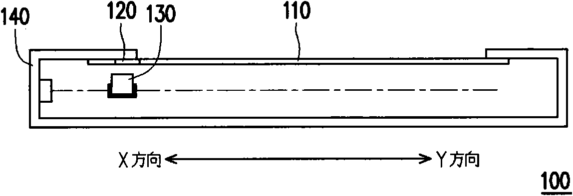
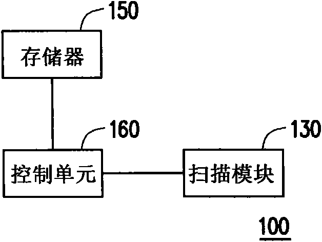
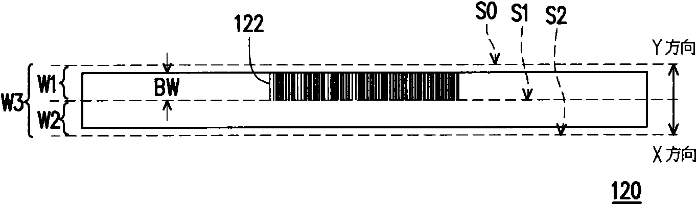
[0049] figure 1 is a schematic cross-sectional view of a scanning device according to an embodiment of the present invention. figure 2 yes figure 1 The circuit block diagram of the scanning device. image 3 is a schematic diagram of a barcode pattern according to an embodiment of the present invention. Please merge reference Figure 1 to Figure 3 . The scanning device 100 may include a flat scanning window 110 , a barcode pattern 122 , a scanning module 130 , a memory 150 and a control unit 160 . The scanning module 130 may include an image sensor and a transmission mechanism (not shown). The image sensor may be a contact image sensor (CIS for short) or a charge coupled device ...
PUM
 Abstract
Description
Claims
Application Information
 - R&D Engineer
- R&D Manager
- IP Professional
- Industry Leading Data Capabilities
- Powerful AI technology
- Patent DNA Extraction
Browse by: Latest US Patents, China's latest patents, Technical Efficacy Thesaurus, Application Domain, Technology Topic, Popular Technical Reports.
© 2024 PatSnap. All rights reserved.Legal|Privacy policy|Modern Slavery Act Transparency Statement|Sitemap|About US| Contact US: help@patsnap.com