Method for fabricating waveguide type surface plasma resonance sensor chip

A surface plasmon and resonance sensor technology, applied in the direction of instruments, scientific instruments, measuring devices, etc., can solve problems such as production difficulties, achieve low cost, and meet the effect of preparation requirements

Inactive Publication Date: 2014-04-16
SUZHOU INST OF NANO TECH & NANO BIONICS CHINESE ACEDEMY OF SCI
View PDF4 Cites 0 Cited by
  • Summary
  • Abstract
  • Description
  • Claims
  • Application Information

AI Technical Summary

Problems solved by technology

However, the traditional chip preparation method is based on the thermal deposition process, and it is difficult to achieve high-efficiency production.

Method used


Image

  • Method for fabricating waveguide type surface plasma resonance sensor chip
  • Method for fabricating waveguide type surface plasma resonance sensor chip
  • Method for fabricating waveguide type surface plasma resonance sensor chip

Examples


Embodiment 1

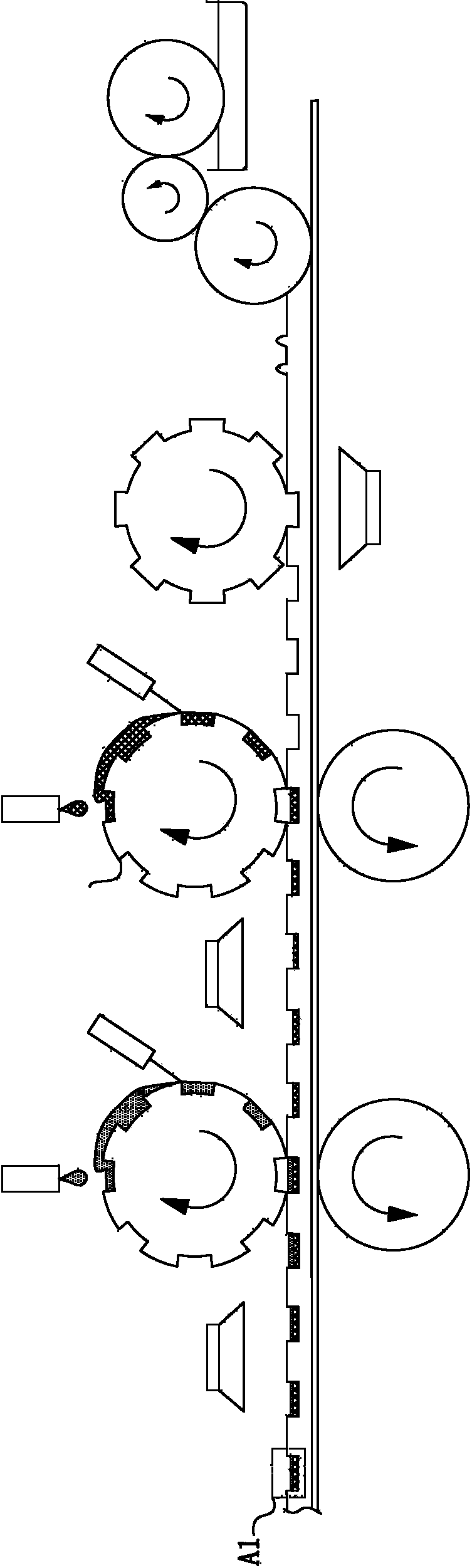
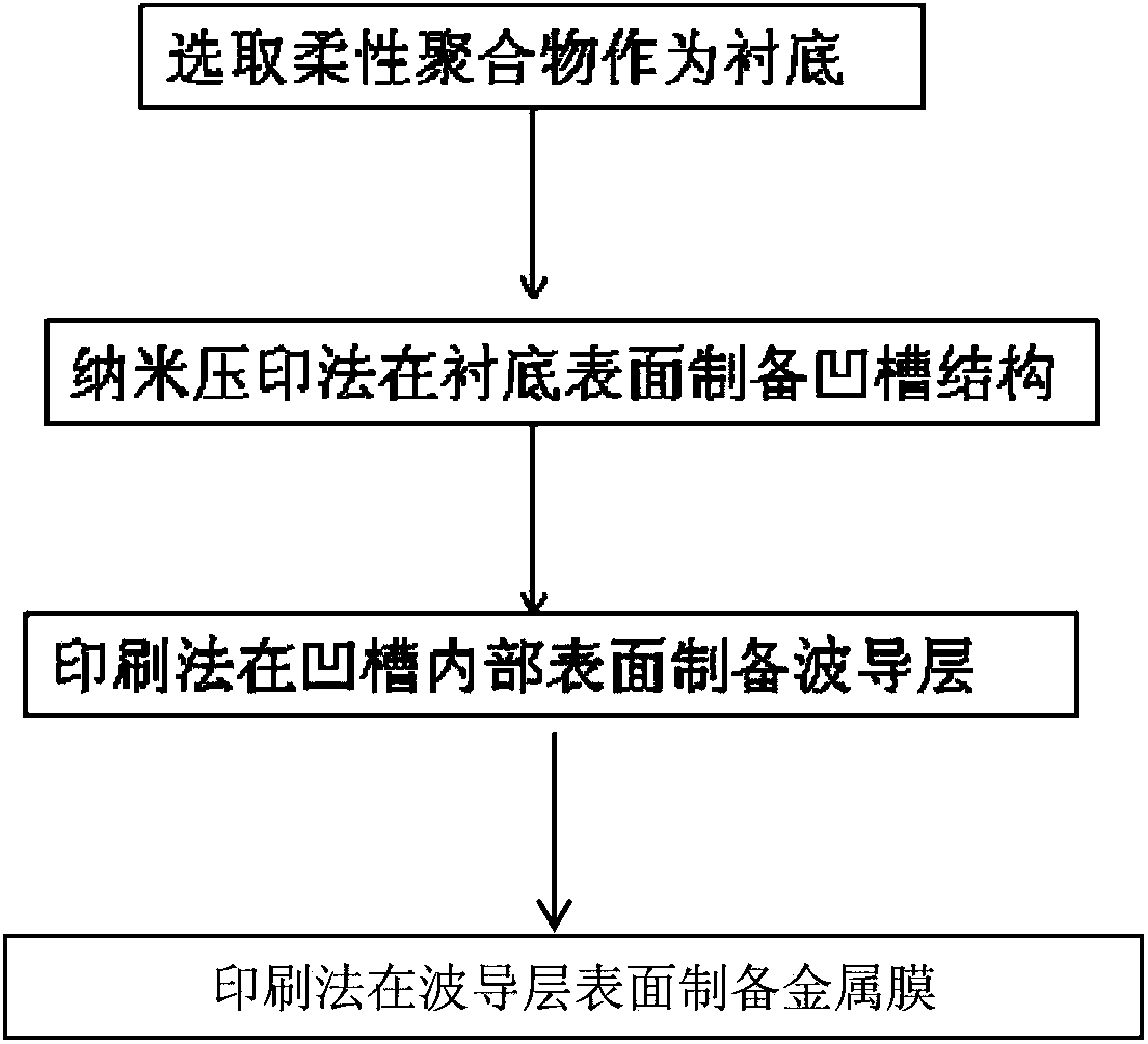
[0027] First, prepare the patterned convex film, waveguide ink, and gold ink. Among them, the waveguide ink has a viscosity of 11-15 s and contains a waveguide polymer with a mass fraction of 10%-25%. In this embodiment, the waveguide ink is a fluorinated polyimide solution with a mass fraction of 10% and a viscosity of 11s. The gold ink is a gold suspension with a mass fraction of 10%. .

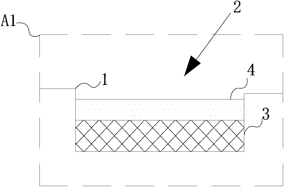
[0028] In the second step, in this embodiment, the roll-to-roll roller imprinting method commonly used in the nanoimprinting method is used to make the groove 2 . The pattern of the convex membrane is imprinted onto the flexible substrate 1 by a nanoimprint method. The groove 2 of the SPR sensor of this embodiment is formed on the flexible substrate 1 . The pattern of the groove 2 is complementary to the pattern of the convex film.

[0029] The third step is the manufacturing process of the waveguide layer 3 . This step is to uniformly print a layer of waveguide material on the bottom ...

Embodiment 2

[0033] The manufacturing steps of this embodiment are different from those of Embodiment 1 in that: in the second step, a planar embossing method is used to manufacture the groove 2 . And polyethylene terephthalate (PET) is selected as the material of the flexible substrate 1 .

[0034] The third step is to use perfluorinated cyclobutyl (PFCB) aryl ether solution with a mass fraction of 12% and a viscosity of 15s as the material of the waveguide ink, and make it into the groove 2 by gravure printing to form a uniform layer A waveguide layer with a thickness of 20 μm.

[0035] The fourth step is to use one of the aluminum suspensions with a mass fraction of 13% as a metal ink to print and form a film. In this embodiment, a metal film 4 made of aluminum with a thickness of 50 nm is formed by accurately spraying to the bottom of the groove 2 by means of gravure printing.

[0036] Please refer to Example 1 for the remaining preparation steps.

Embodiment 3

[0038] The manufacturing steps of this embodiment are different from those of Embodiment 1 in that: in the second step, a planar embossing method is used to manufacture the groove 2 . And polyethylene terephthalate (PEN) is selected as the material of the flexible substrate 1 . The third step is to use a halogenated polyacrylate solution with a mass fraction of 15% and a viscosity of 13s as the waveguide ink, and make it into the groove 2 by aerosol jet printing to form a uniform waveguide layer with a thickness of 30 μm. . The fourth step is to use the copper suspension with a mass fraction of 15% as the metal ink to print the film. In this embodiment, aerosol spray printing is used to accurately print to the bottom of the groove 2 to form a copper metal film 4 with a thickness of 70 nm.

[0039] Please refer to Example 1 for the remaining preparation steps.

[0040] In other embodiments, the flexible substrate 1 is made of some high refractive index organic polymers, such...


PUM

PropertyMeasurementUnit
thicknessaaaaaaaaaa
thicknessaaaaaaaaaa

Abstract

The invention provides a method for fabricating a waveguide type surface plasma resonance sensor chip, comprising the steps of: preparing a patterned convex membrane and metal ink; pressing patterns of the convex membrane onto a flexible substrate by using a nano-pressing method so that grooves corresponding to the patterns are formed on the flexible substrate; and printing a film in the grooves by using the metal ink. The method provided by the invention is suitable for fabricating the waveguide type surface plasma resonance sensor chip; and according to the method, the process is simple, and the sensor chips are produced in a large area and a large scale with low cost, and besides, the fabrication demands of the sensor chips can be satisfied and the actual requirements at present can be met well.

Description

technical field [0001] The invention relates to the field of sensor manufacturing, in particular to a method for making a sensor chip by using nano-imprinting or printing technology. Background technique [0002] The surface plasmon resonance sensor is the product of the intersection of physics and biological science. The surface plasmon resonance sensor can be used to analyze the interaction between various biomolecules, such as: DNA-DNA, antigen and antibody, DNA and Protein and other biomolecular interactions. The surface plasmon resonance sensor has become a very important instrument and equipment in life science research. The surface plasmon resonance sensor system is composed of a chip, an optical system and a signal detection system. [0003] The waveguide surface plasmon resonance sensor has less research, but the advantage of the waveguide surface plasmon resonance sensor chip is that it can control the propagation of the optical path, and it is easy to integrate w...

Claims


Application Information

Patent Timeline
Patent Type & Authority Patents(China)
IPC IPC(8): G01N21/55G01N21/552
Inventor 潘革波李岩肖燕
Owner SUZHOU INST OF NANO TECH & NANO BIONICS CHINESE ACEDEMY OF SCI
Why Eureka
Try Eureka