Single-electron transistor using nanoparticles

a single-electron transistor and nanoparticle technology, applied in the field of single-electron transistors, can solve the problems of not being suitable for commercial applications requiring mass production, difficult to form a small channel enough to be used at room temperature,

Inactive Publication Date: 2006-01-10
SAMSUNG ELECTRONICS CO LTD
View PDF4 Cites 7 Cited by
  • Summary
  • Abstract
  • Description
  • Claims
  • Application Information

AI Technical Summary

Benefits of technology

[0014]According to the present invention, previously prepared nanoparticles are used as channels. Therefore, a channel narrow enough for operation at

Problems solved by technology

However, with respect to the photolithography, it is difficult to form a small channel enough to be used at room temperature.
The e-beam lithogr

Method used


Image

  • Single-electron transistor using nanoparticles
  • Single-electron transistor using nanoparticles
  • Single-electron transistor using nanoparticles

Examples


first embodiment

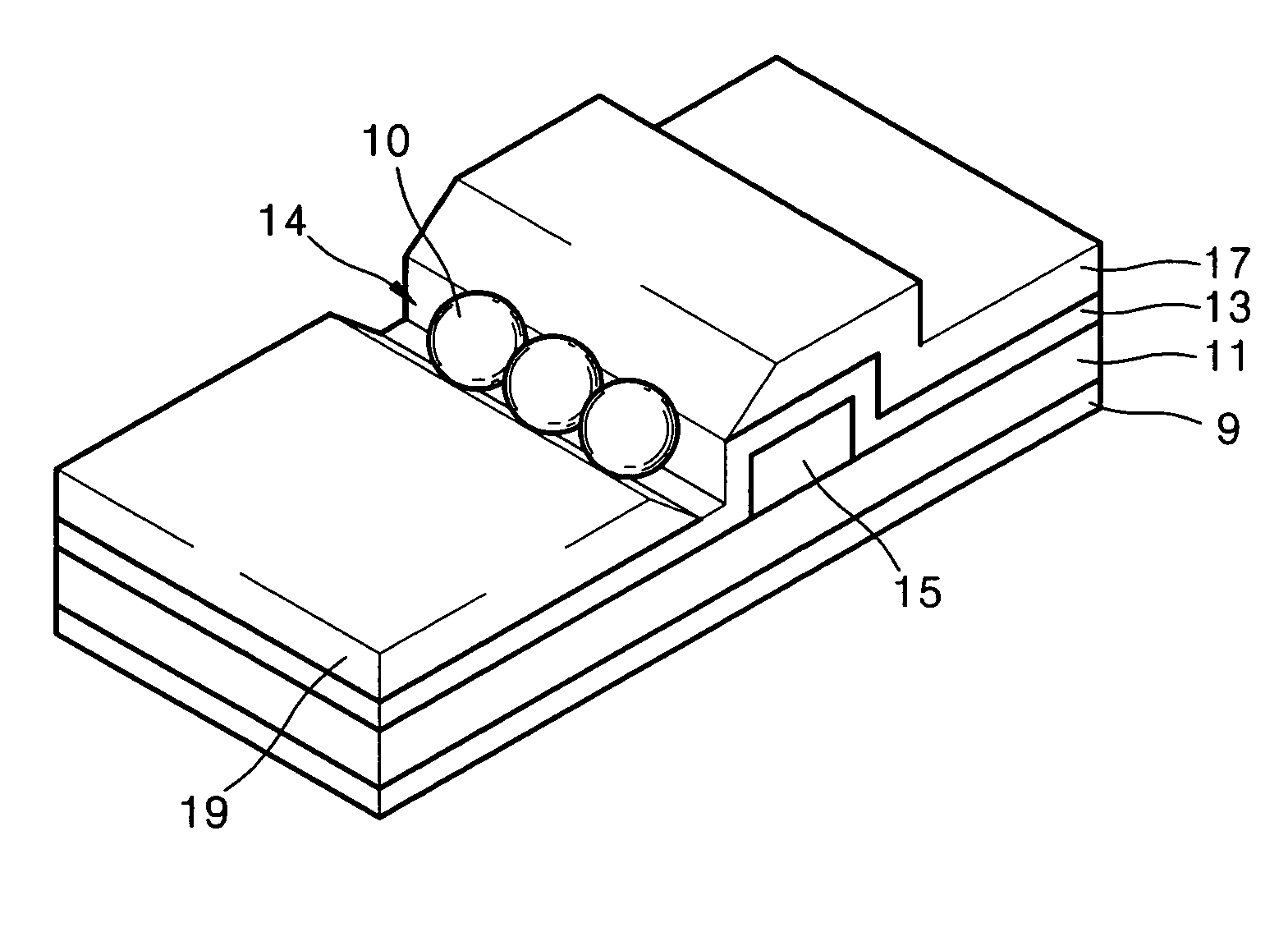
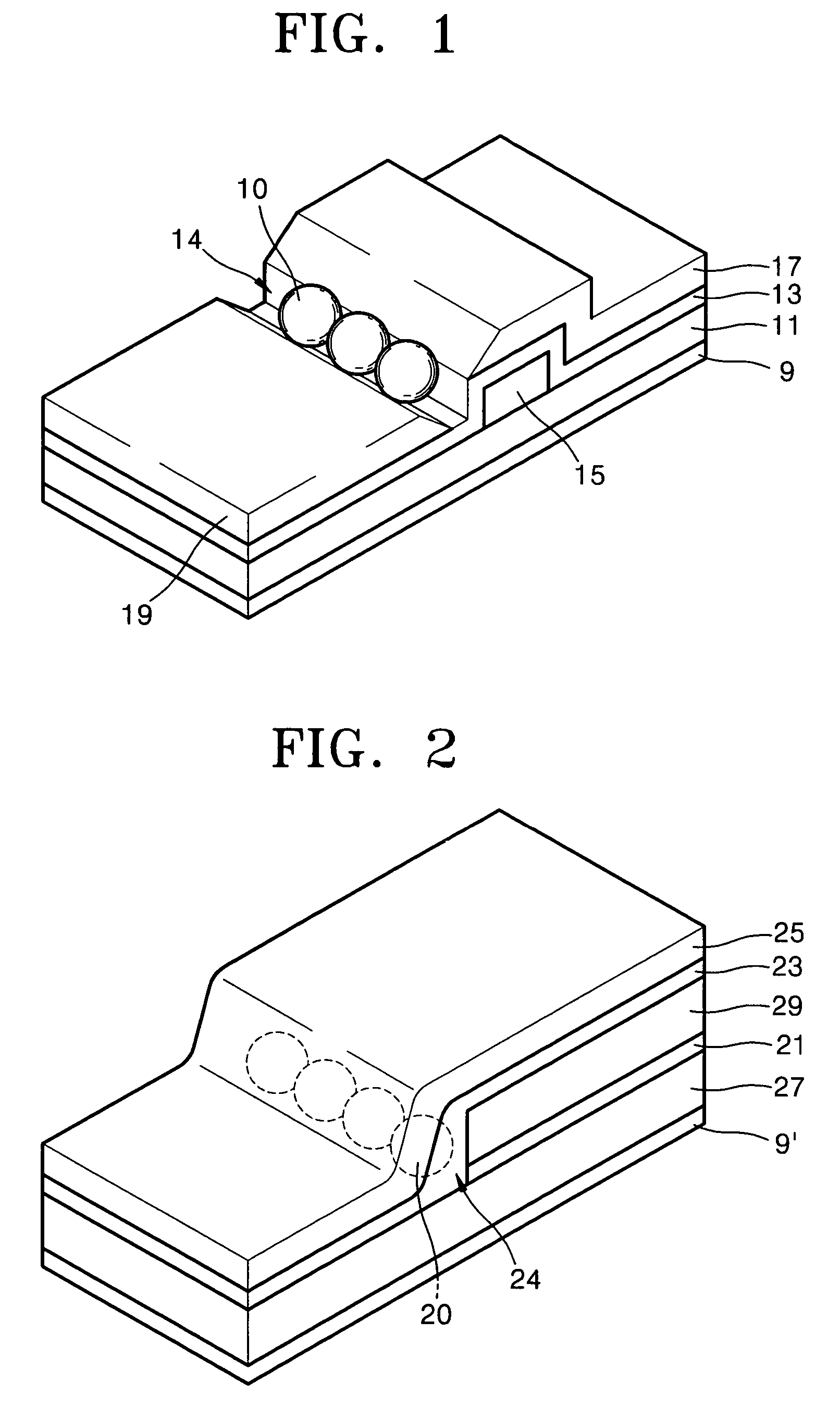
[0024]FIG. 1 is a perspective view of a single-electron transistor using nanoparticles according to the present invention.

[0025]Referring to FIG. 1, the single-electron transistor according to the first embodiment of the present invention comprises a substrate 9, a first insulating film 11 formed on the substrate 9, a gate electrode 15 patterned in a stripe form of a predetermined width on the first insulating film 11, and a second insulating film 13 formed on exposed surfaces of the first insulating film 11 and the gate electrode.

[0026]A metal layer is deposited on the second insulating film 13 by sputtering or evaporation. A groove 14 is formed at a stepped portion, i.e., at a boundary of the first insulating film 11 and the gate electrode 15 to expose a surface of the second insulating film 13. As a result, the metal layer is separated into two regions to thereby serve as a source electrode 19 and a drain electrode 17.

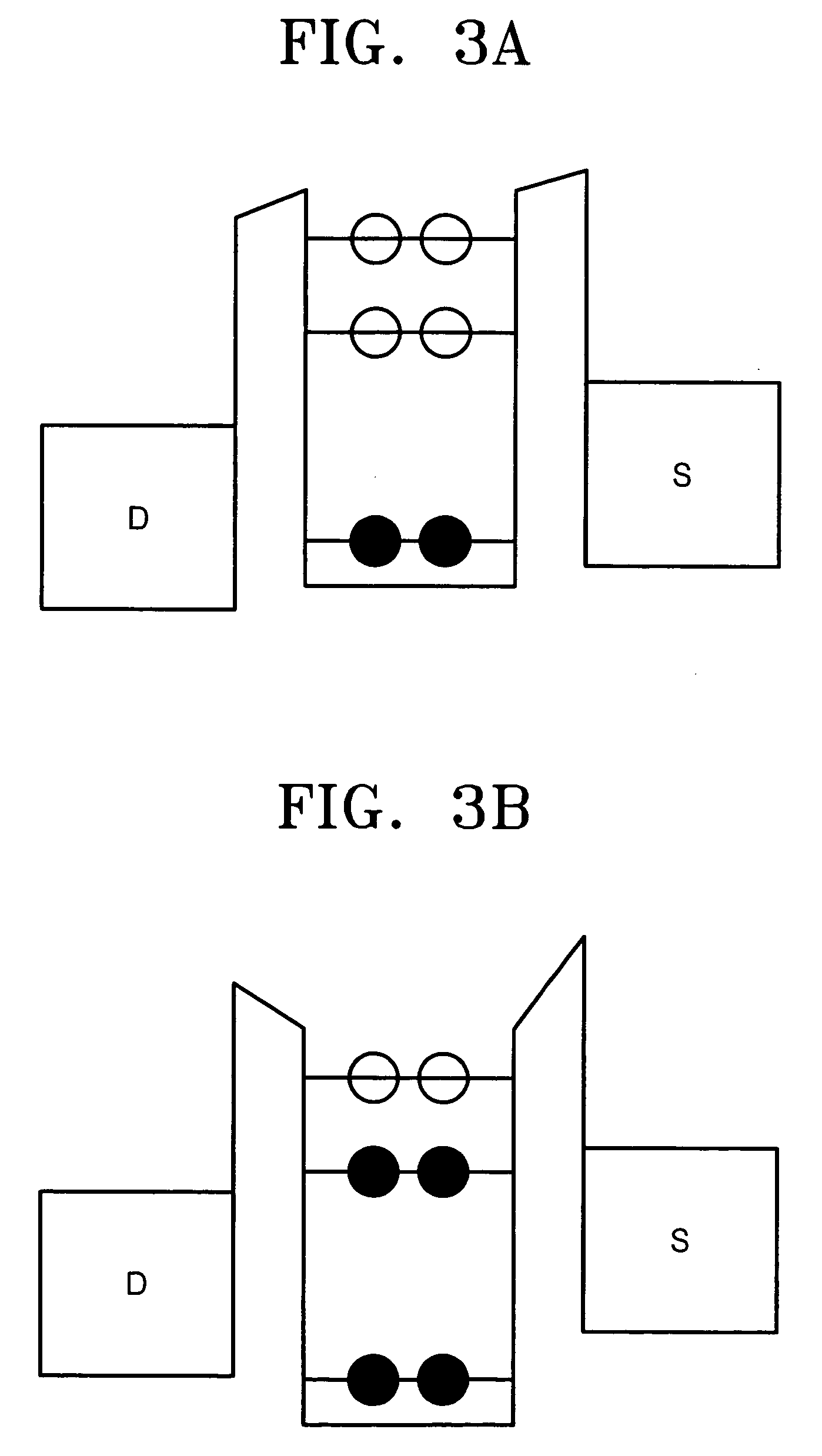
[0027]Nanoparticles 10 previously prepared in a physical or ch...


PUM


Abstract

A single-electron transistor using nanoparticles is provided. The single-electron transistor includes a first insulating film, a gate electrode patterned in a stripe form on the first insulating film, a second insulating film formed on exposed surfaces of the first insulating film and the gate electrode in such a way that a stepped portion is formed at a boundary between the gate electrode and the first insulating film, first and second electrodes formed on the second insulating film in such a way that a groove is formed at the stepped portion to expose a surface of the second insulating film, the first and second electrodes being separated from each other by the groove, and nanoparticles positioned at the groove and contacting with the first and second electrodes, the nanoparticles being channels for electron transfer. The single-electron transistor is manufactured using previously prepared nanoparticles and a general semiconductor process, thereby enabling low cost, mass production and operation at room temperature.

Description

BACKGROUND OF THE INVENTION[0001]1. Field of the Invention[0002]The present invention relates to a single-electron transistor, and more particularly, to a single-electron transistor using nanoparticles.[0003]2. Description of the Related Art[0004]A single-electron transistor is a device that uses one electron to control a current by Coulomb blockade. The Coulomb blockade means a phenomenon that tunneling of an electron into a dot is blocked by a Coulomb repulsive interaction of it with another electron previously present in the dot.[0005]Generally, current-voltage characteristics of a tunnel junction having a size of less than 100 nm and an appropriate resistance level do not follow Ohm's law. Rather, a current generated by tunneling of an electron at a low voltage approximates to zero. This phenomenon is generated by an electrostatic interaction of a tunneling electron and a charged medium. A theory based on quantum mechanics explains the phenomenon (for example, see Likharev et al...

Claims


Application Information

Patent Timeline
IPC IPC(8): H01L29/78H01L29/775H01L21/335H01L29/76
CPCB82Y10/00H01L29/7613H01L29/66439Y10S977/937H01L29/775
Inventor KHANG, YOON-HO
Owner SAMSUNG ELECTRONICS CO LTD
Why Eureka
Try Eureka