Al technical title is built by PatSnap Al team. It summarizes the technical point description of the patent document.
a transparent, conducting electrode technology, applied in the field of optoelectronic devices, can solve the problems of increasing the cost of manufacturing, so as to achieve the effect of relatively inexpensive and large-scale production
Inactive Publication Date: 2009-09-29
AERIS CAPITAL SUSTAINABLE IP
View PDF41 Cites 50 Cited by
Summary
Abstract
Description
Claims
Application Information
AI Technical Summary
This helps you quickly interpret patents by identifying the three key elements:
Problems solved by technology
Method used
Benefits of technology
[0013]Embodiments of the present invention provide new and useful optoelectronic devices that may be formed relatively inexpensively and on a large scale.
Problems solved by technology
The drawback of this approach is that metal oxides are not proper conductors, with sheet resistance typically being at least 5 Ohms / □ for the most expensive products and often more than 60-200 Ohms / □ for lower-priced materials.
As a result, there is currently a tradeoff when integrating lower-cost, high-resistivity conducting glasses into optoelectronic devices, with higher resistance translating into significant energy losses in several applications.
The alternative strategy of employing significantly more expensive, incrementally more conductive glasses, often with still unsatisfying resistivity, leads to a limited adoption of otherwise market-competitive products.
Thus, expensive TCEs represent a bottleneck in the development of inexpensive optoelectronic products; in many cases, the TCEs are currently the primary cost contributor within a complex device (e.g. solar cells, LEDs).
Method used
Image
Click on the blue label to locate the original text in one second.
Reading with bidirectional positioning of images and text.
Examples
Embodiment Construction
Contents
I. Glossary
II. General Overview
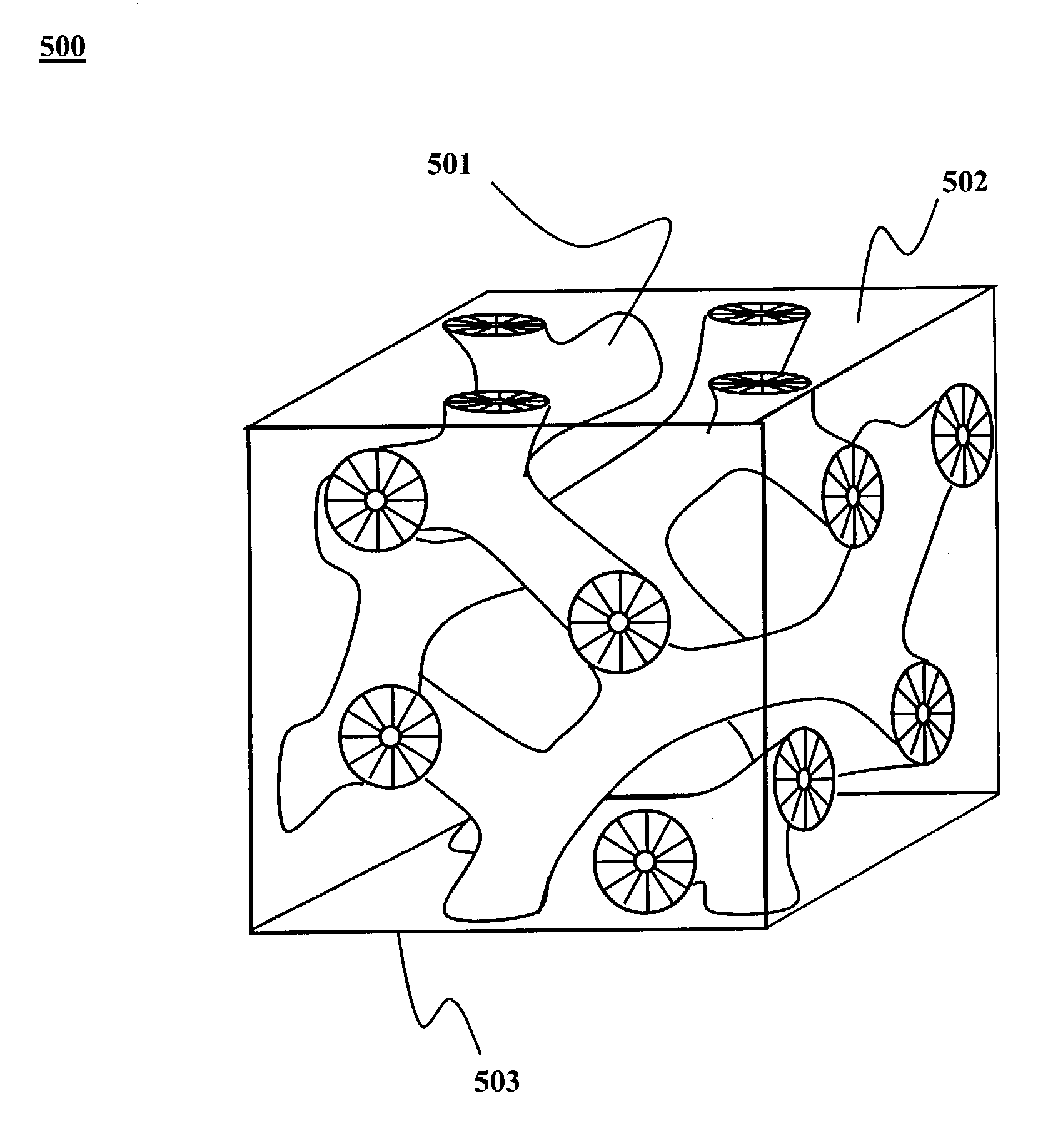
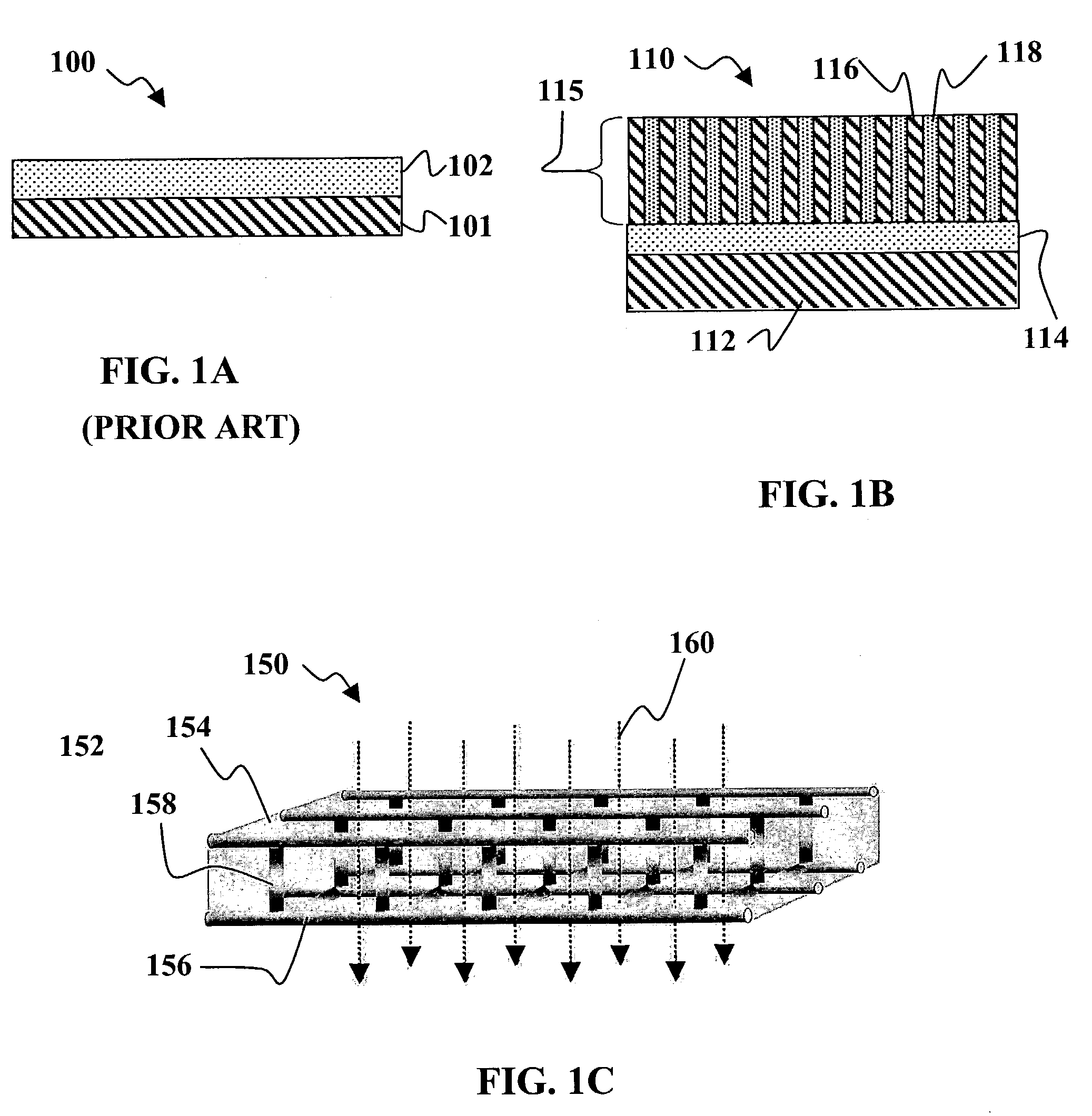
III. Nanostructured Transparent Conducting Electrodes
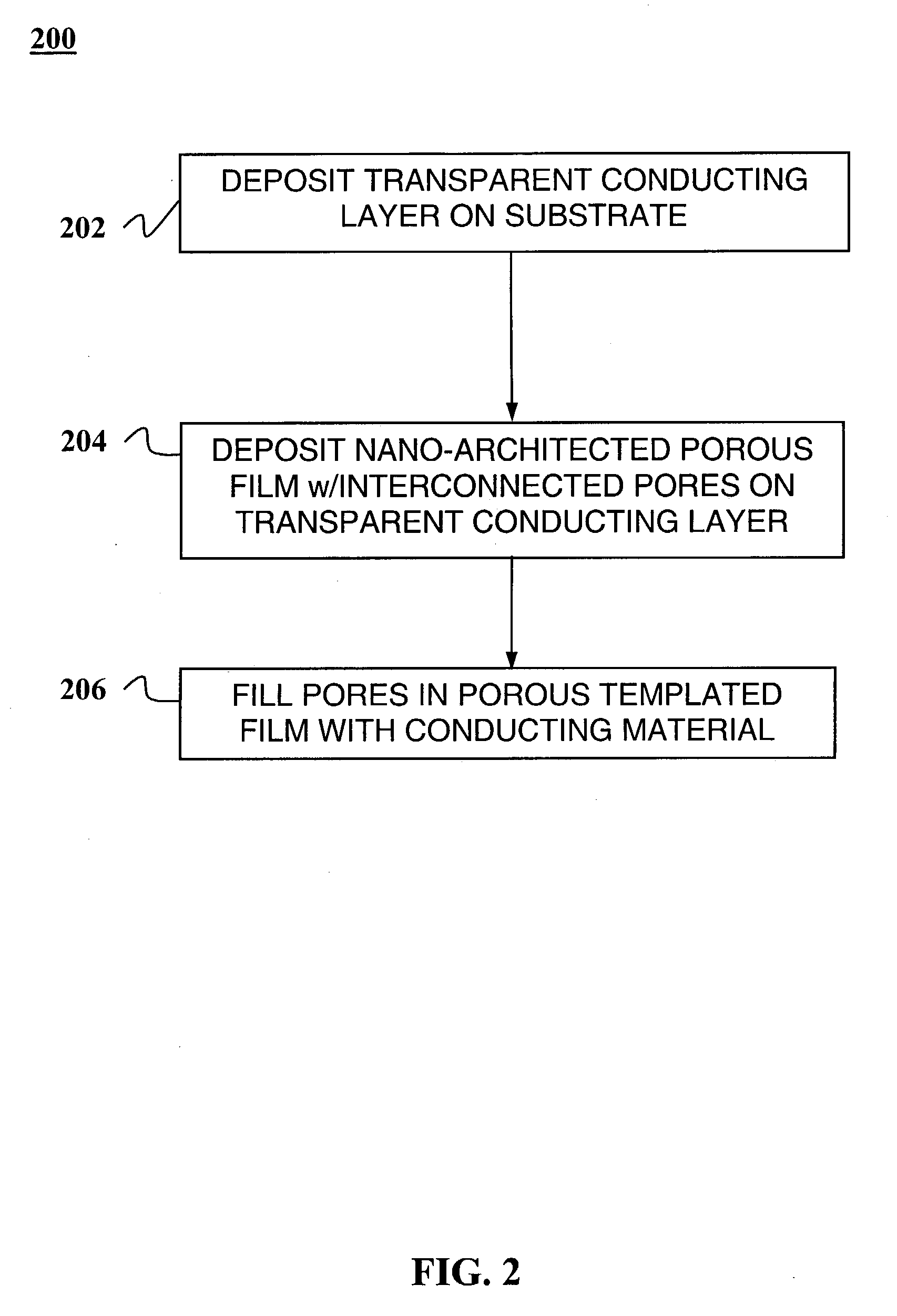
IV. Fabrication of Nanostructured Transparent Conducting Electrodes
V. Devices using Nanostructured Transparent Conducting Electrodes
VI. Alternative Embodiments
VII. Conclusion
I. GLOSSARY
[0031]The following terms are intended to have the following general meanings as they are used herein:
Device: An assembly or sub-assembly having one or more layers of material.
Semiconductor: As used herein, semiconductor generally refers to a material characterized by an electronic bandgap typically between about 0.5 eV and about 3.5 eV.
[0032]Hole-Acceptor, Electron-Acceptor: In the case of semiconductor materials, hole-acceptor and electron-acceptor are relative terms for describing charge transfer between two materials. For two semiconductor materials wherein a first material has a valence band edge or highest occupied molecular orbital (HOMO) that is higher than the corresponding valence band edge or HOMO fo...
PUM
Property
Measurement
Unit
diameters
aaaaa
aaaaa
diameters
aaaaa
aaaaa
diameter
aaaaa
aaaaa
Abstract
Transparent conducting electrodes, methods for manufacturing such conducting electrodes, optoelectronic devices incorporating such transparent electrodes and methods for making such optoelectronic devices and solar power generation systems incorporating such electrodes are disclosed. Nanostructured transparent conducting electrodes may include a nano-architected porous film having a network of ordered interconnected pores and an electrically conductive material that substantially fills the pores. The nano-architected porous film may be disposed on a layer of transparent conducting material. The electrode may include a substrate (e.g., glass or polymer) and the layer of transparent conducting material may be disposed between the substrate and the nano-architected porous film. Nanostructured transparent conducting electrodes may be fabricated by forming a nano-architected porous film, e.g., by surfactant temptation, on a layer of transparent conducting material and substantially filling the pores in the nano-architected porous film with an electrically conductive material, e.g., by electrodeposition. Optoelectronic devices may incorporate one or more nanostructured transparent conducting electrodes in electrical contact with an active layer. Such devices may be made by fabricating a first electrode and disposing an active layer between the first electrode and a second electrode, one of which is a nanostructured transparent conducting electrode.
Description
CROSS-REFERENCE TO AN EARLIER FILED APPLICATION[0001]This application is a continuation-in-part of co-pending U.S. patent application Ser. No. 10 / 303,665, now U.S. Pat. No. 7,253,017, filed Nov. 22, 2002, and a continuation-in-part of U.S. patent application Ser. No. 10 / 319,406, now U.S. Pat. No. 6,852,920, filed Dec. 11, 2002. Application Ser. Nos. 10 / 303,665,10 / 319,406 and this application claim priority to U.S. Provisional Patent Application 60 / 390,904, filed Jun. 22, 2002. This application is also a continuation-in-part of U.S. patent application Ser. No. 10 / 290,119, now U.S. Pat. No. 7,291,782, filed Nov. 5, 2002. The entire disclosures of applications of Ser. Nos. 10 / 303,665, 10 / 319,406, 60 / 390,904 and 10 / 290,119 are incorporated herein by reference.FIELD OF THE INVENTION[0002]This invention generally relates to optoelectronic devices and more particularly to photovoltaic, e.g., solar cell, devices.BACKGROUND OF THE INVENTION[0003]Conducting glasses are indispensable in many o...
Claims
Application Information
Patent Timeline
Application Date:The date an application was filed.
Publication Date:The date a patent or application was officially published.
First Publication Date:The earliest publication date of a patent with the same application number.
Issue Date:Publication date of the patent grant document.
PCT Entry Date:The Entry date of PCT National Phase.
Estimated Expiry Date:The statutory expiry date of a patent right according to the Patent Law, and it is the longest term of protection that the patent right can achieve without the termination of the patent right due to other reasons(Term extension factor has been taken into account ).
Invalid Date:Actual expiry date is based on effective date or publication date of legal transaction data of invalid patent.