Optoelectronic fiber

a technology of optoelectronic fiber and fiber, which is applied in the direction of filament/thread forming, thermoelectric devices, and control devices. it can solve the problems of unattractive unfavorable large-scale energy production of solar cells, and inability to meet the needs of large-scale production, etc., and achieves the effect of relatively inexpensive and large-scale production

Inactive Publication Date: 2009-05-19
AERIS CAPITAL SUSTAINABLE IP
View PDF66 Cites 49 Cited by
  • Summary
  • Abstract
  • Description
  • Claims
  • Application Information

AI Technical Summary

Benefits of technology

[0009]Embodiments of the present invention provide new and useful optoelectronic materials that may be formed relatively inexpensively and on a large scale.

Problems solved by technology

Unfortunately, such solar cells are currently made in the form of thin sheets or panels.
Such panels are typically rigid, expensive, and delicate and may degrade under prolonged exposure to the elements.
This makes solar cells unattractive for large-scale energy production.
Unfortunately, no solar cell fiber presently exists.

Method used


Image

  • Optoelectronic fiber
  • Optoelectronic fiber
  • Optoelectronic fiber

Examples


Embodiment Construction

Contents

I. Glossary

II. General Overview

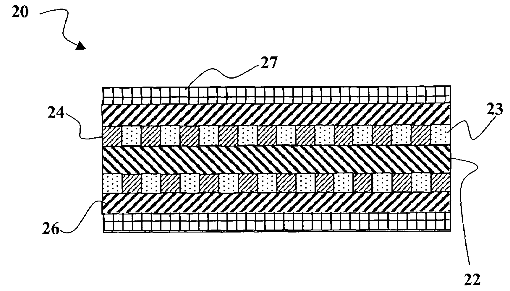
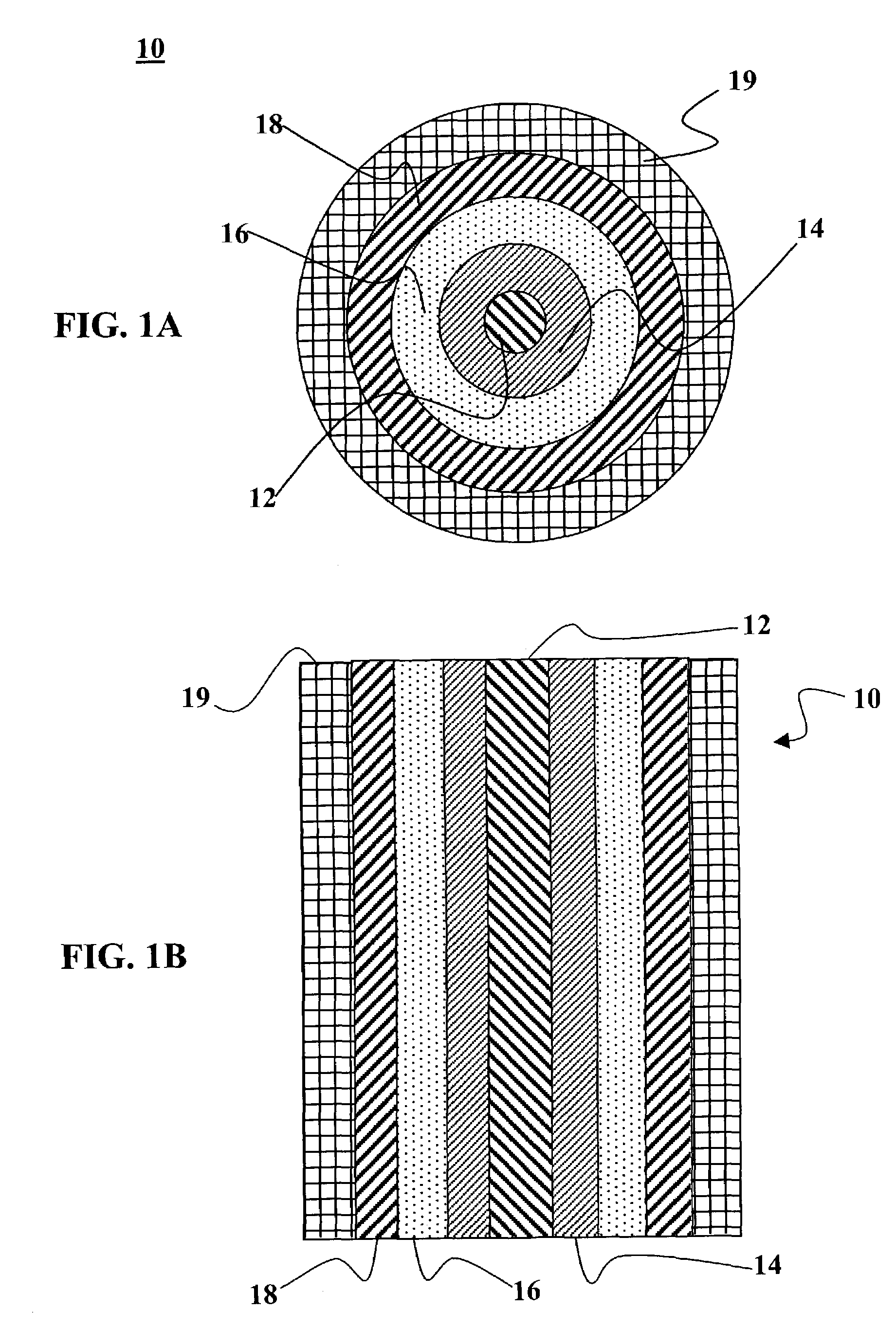
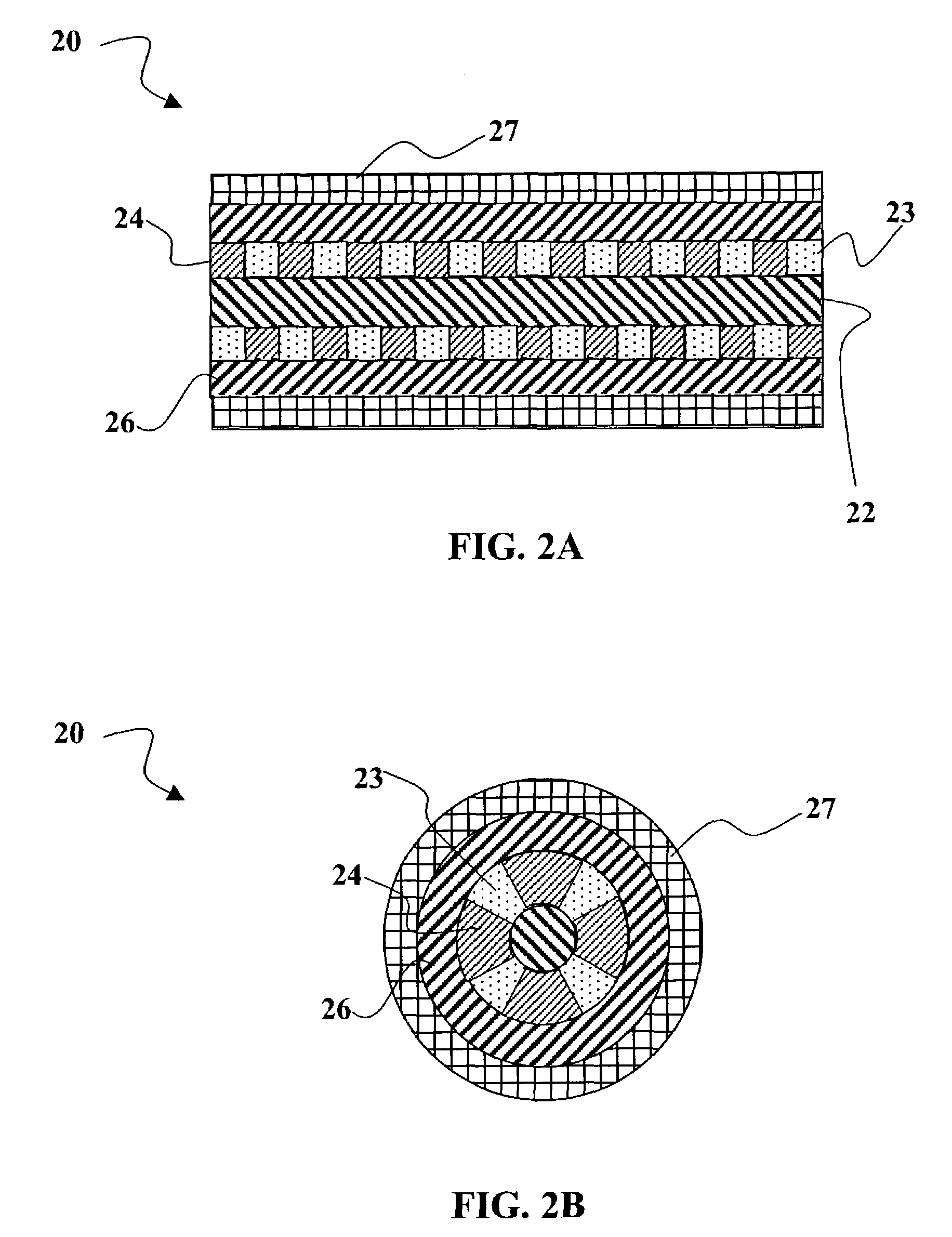
III. Optoelectronic Fiber Architecture

IV. Fabrication of Optoelectronic Fibers

V. Alternative Embodiments

VI. Conclusion

I. GLOSSARY

[0017]The following terms are intended to have the following general meanings as they are used herein:

Electrospinning: In general, electrospinning refers to a process for forming threads or fibers from a spinning solution by passing the solution into an electric field in a thin stream or in drops on order to separate the stream or drops into threads.

Device: An assembly or sub-assembly having two or more layers of material.

[0018]Semiconductor: As used herein, semiconductor generally refers to a material characterized by an electrical conductivity that depends strongly on material properties and other factors. Material properties may include crystalline orientation and the presence of dopants. Other factors may include temperature, applied electric field, incident radiation, and the like.

N-type semiconductor, P-type sem...


PUM

PropertyMeasurementUnit
diameteraaaaaaaaaa
diameteraaaaaaaaaa
diameteraaaaaaaaaa

Abstract

An optoelectronic fiber and methods for forming such a fiber are disclosed. The fiber generally includes an electrically conductive fiber core, a first semiconducting layer substantially surrounding the fiber core, and a second semiconducting layer substantially surrounding the first semiconducting layer. The first and second semiconducting layers are of complementary types, i.e., one is p-type and the other is n-type. The fiber may be made, e.g., by electrospinning a material to form a fiber core; substantially surrounding the fiber with a first semiconducting material; and substantially surrounding the first semiconducting material with a second semiconducting material. Optoelectronic fibers can be fashioned into a web to provide a solar cell material or substantially transparent conductive material.

Description

FIELD OF THE INVENTION[0001]This invention generally relates to photovoltaic devices and more particularly to solar cell devices formed on a fiber.BACKGROUND OF THE INVENTION[0002]Approximately 1000 Watts of power in the form of solar radiation strike each square meter of the Earth's surface. Means for converting this solar energy into useful electricity, often referred to as solar cells, are well known. Unfortunately, such solar cells are currently made in the form of thin sheets or panels. Such panels are typically rigid, expensive, and delicate and may degrade under prolonged exposure to the elements. This makes solar cells unattractive for large-scale energy production. It would be greatly advantageous to provide solar cells in the form of a flexible, portable, versatile, light-weight, and multifunctional material that can be used to make energy-producing electronic textiles for clothing, tent material, sail material, and energy producing fabrics that can cover a wide variety of...

Claims


Application Information

Patent Timeline
Patent Type & Authority Patents(United States)
IPC IPC(8): H01L31/0336H01L31/042
CPCD01D5/34H01L31/0322H01L31/035281Y02E10/541
Inventor SAGER, BRIAN M.ROSCHEISEN, MARTIN R.
Owner AERIS CAPITAL SUSTAINABLE IP
Why Eureka
Try Eureka