Measuring method and apparatus of thin film thickness

a thin film and thickness technology, applied in the direction of instruments, resistance/reactance/impedence, electric/magnetic measuring arrangements, etc., can solve the problem of difficult film thickness measurement over a wide range, and achieve the effect of large-scal

Inactive Publication Date: 2005-04-07
HITACHI PLANT TECH LTD
View PDF3 Cites 52 Cited by
  • Summary
  • Abstract
  • Description
  • Claims
  • Application Information

AI Technical Summary

Benefits of technology

An object according to the present invention is to provide a method for measuring the thickness of such the thin film formed through or putting the conductive layer therebetween, enabling the measurement protecting from an error thereof due to the curve and / or the winding on the surface of a substrate and / or a stage, but without necessitating a large-scaled facility, and also enabling to grasp the minute surface configurations covering over a wide range.

Problems solved by technology

With such the contact-type step meter relating to the conventional art mentioned above, however, there is a problem; i.e., principally, it is difficult to make the measurement on the film thickness over the wide range thereof.

Method used


Image

  • Measuring method and apparatus of thin film thickness
  • Measuring method and apparatus of thin film thickness
  • Measuring method and apparatus of thin film thickness

Examples


Embodiment Construction

Hereinafter, embodiments according to the present invention will be fully explained by referring to the drawings attached herewith.

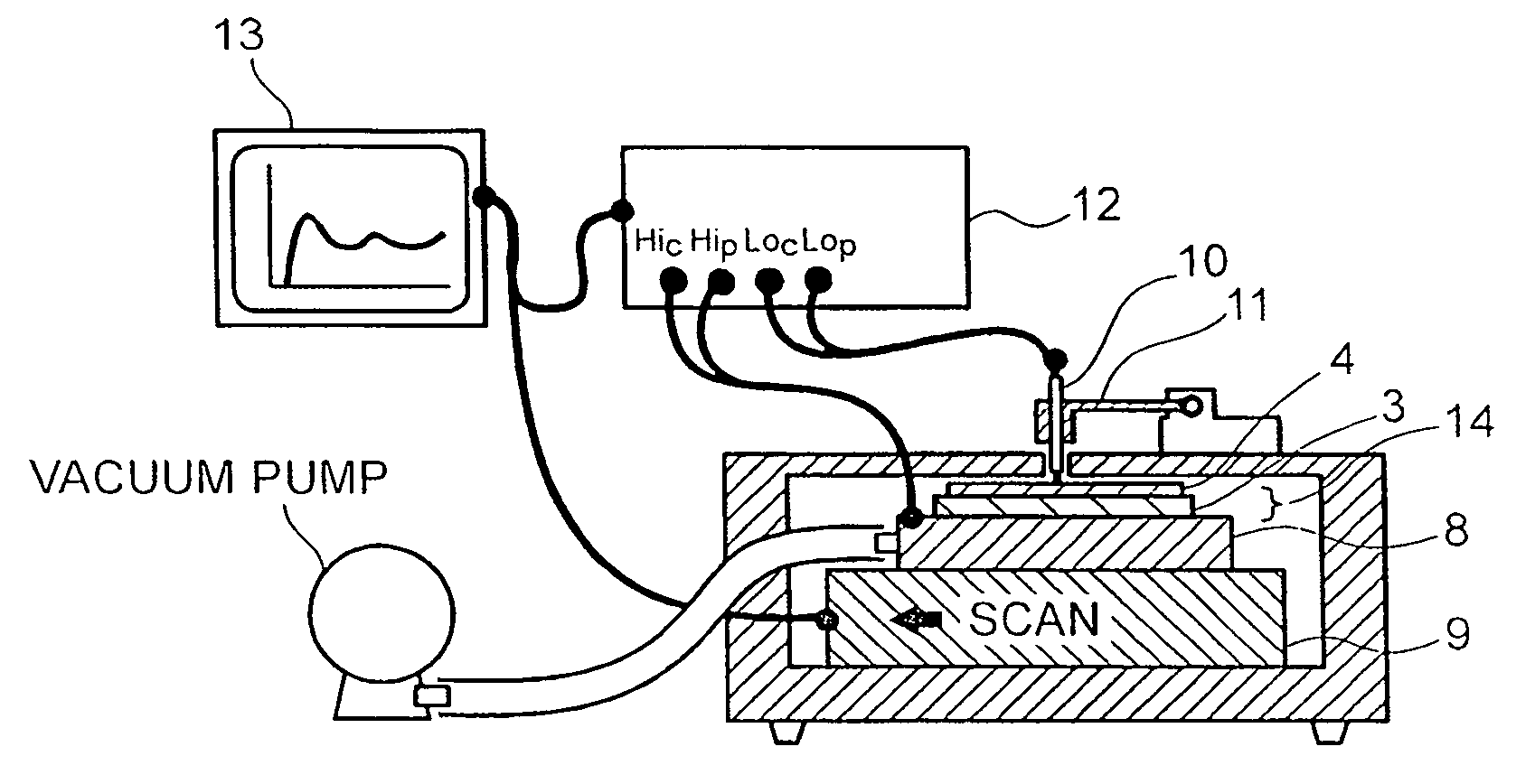
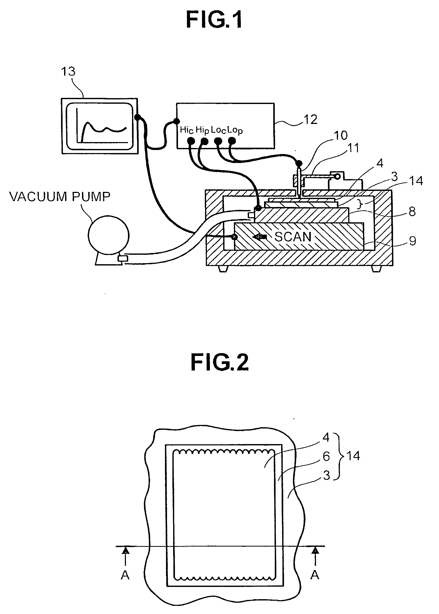
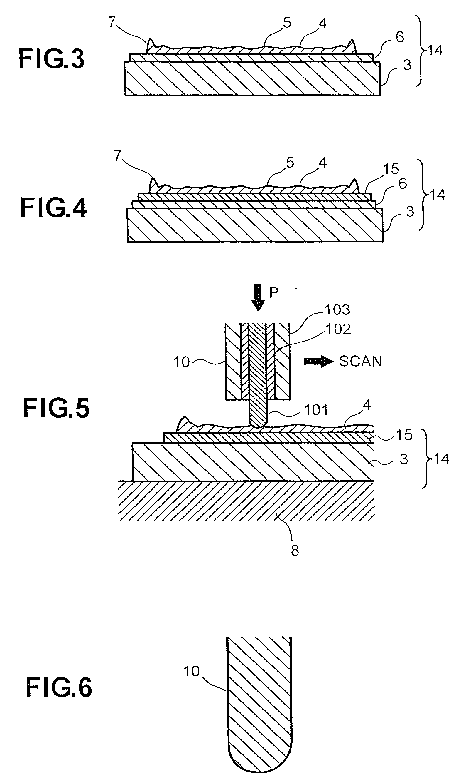
FIG. 1 is a schematic structural view for showing an entire of an apparatus for measuring thickness of a thin film, according to an embodiment of the present invention. In this FIG. 1, a substrate 3 and a thin film 4 formed thereon through or putting a transparent film therebetween (not shown in the figure), forming a target 14 to be measured (hereinafter, “measuring target”), they are mounted on a wafer stage made of a conductor, while being absorbed through vacuum.

Those of the substrate 3, the measuring target 14 and the wafer stage 8 are provided on an x-y stage 9. On the other hand, a probe 10 is attached at a tip portion of a cantilever 11, and it is in contact with the thin film 4 upon the surface thereof, due to the gravity acting thereon. The probe 10 and the wafer stage 8 are connected to LCR meter 12, respectively. Applying an electric fiel...


PUM


Abstract

In an apparatus for measuring thickness of a thin film, which is formed through a conductor, preventing the measurement from an error due to the curve or bend on a substrate surface or a moving surface of a stage, but without necessity of a large-scaled facility, an electric filed is applied between a probe 10 and a stage 8, so as to obtain an electrostatic capacitance of the substrate 3, an electrostatic capacitance of an insulating film, which is formed between the substrate 3, and an electrostatic capacitance defined starting from the substrate 3 to the thin film 4. The electrostatic capacitance between the substrate 3 and the thin film 4 is measured at plural numbers of places covering over the entire surface of the thin film 4. The probe 10 is so supported that the contact load “P” comes to be constant, by the probe 10 onto the thin film 4. A contact area of the probe 10 between the thin film 4 is calculated out through a predetermined equation, assuming the load “P” is constant. From respective electrostatic capacitances and the contact area measured, a distribution of thickness of the thin film 4 over the entire area thereof.

Description

BACKGROUND OF THE INVENTION The present invention relates to a method and an apparatus for measuring thickness of a thin film, and it relates, in particular, to a measuring method and an apparatus thereof, for making a measurement on a thin film formed upon a semiconductor substrate and / or a glass substrate for use of a flat display panel, etc., through or putting a conductive layer of a transparent electrode therebetween, about the thickness and a distribution thereof. In the field of semiconductors or flat display panels, such as thin-film structures made of a dielectric substance are applied many, into the structures and the manufacturing processes thereof; for example, a photo resist, an orientation film for controlling an orientation of a liquid crystal, a color filter, a transportation layer of electrons or holes, a light emission layer, etc. Conventionally, those thin-film structures are manufactured by forming a film through a vacuum process and / or a spin coating process,...

Claims


Application Information

Patent Timeline
Patent Type & Authority Applications(United States)
IPC IPC(8): G01B7/06G01R27/26H01L21/66
CPCG01R27/2605
Inventor KOHNO, RYUJINAGATA, TATSUYAWATASE, NAOKIWATANABE, MICHIHIRO
Owner HITACHI PLANT TECH LTD
Why Eureka
Try Eureka