Thin film transistor substrate having transparent conductive metal and method of manufacturing the same

a technology substrates, applied in transistors, optics, instruments, etc., can solve the problems of increasing material costs, affecting the production efficiency of thin film transistors, and tft using polysilicon has difficulty in achieving a large scale, etc., to achieve simplified manufacturing process, high resolution, and large scale

Inactive Publication Date: 2011-04-12
SAMSUNG DISPLAY CO LTD
View PDF7 Cites 49 Cited by
  • Summary
  • Abstract
  • Description
  • Claims
  • Application Information

AI Technical Summary

Benefits of technology

[0011]The present invention provides a thin film transistor, a thin film transistor substrate and a method of manufacturing the same, where high resolution and large scale can be provided and a manufacturing process can be simplified.

Problems solved by technology

However, the TFT using the polysilicon has difficulty in achieving a large scale due to its poor uniformity and needs a high temperature process.
When the source / drain electrodes are formed of the transparent electrodes and a large area is covered, the resistance rises to bring about a considerable signal delay.
Moreover, when the source / drain electrodes are formed of Au, the material cost is increased.

Method used


Image

  • Thin film transistor substrate having transparent conductive metal and method of manufacturing the same
  • Thin film transistor substrate having transparent conductive metal and method of manufacturing the same
  • Thin film transistor substrate having transparent conductive metal and method of manufacturing the same

Examples


Embodiment Construction

[0024]Exemplary embodiments of the present invention are described with reference to the accompanying drawings in detail. The same reference numbers are used throughout the drawings to refer to the same or like parts. Detailed descriptions of well-known functions and structures incorporated herein are omitted to avoid obscuring the subject matter of the present invention.

[0025]The present invention may be embodied in many different forms. Specific embodiments of the invention are shown in drawings and described herein in detail, and it is understood that the present disclosure does not limit the invention to the specific embodiments illustrated.

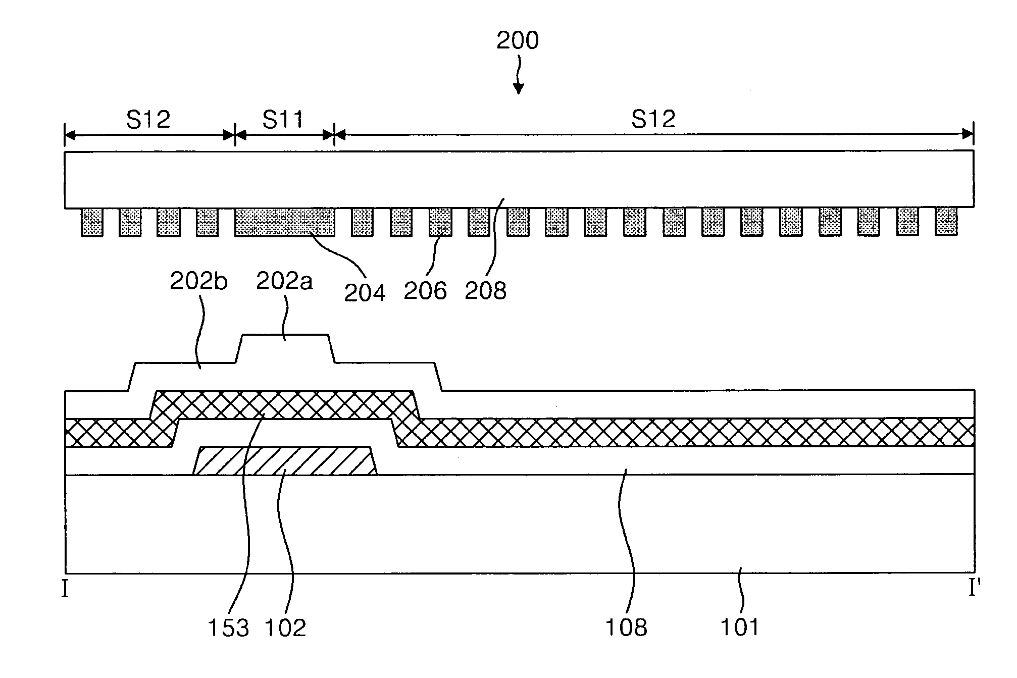
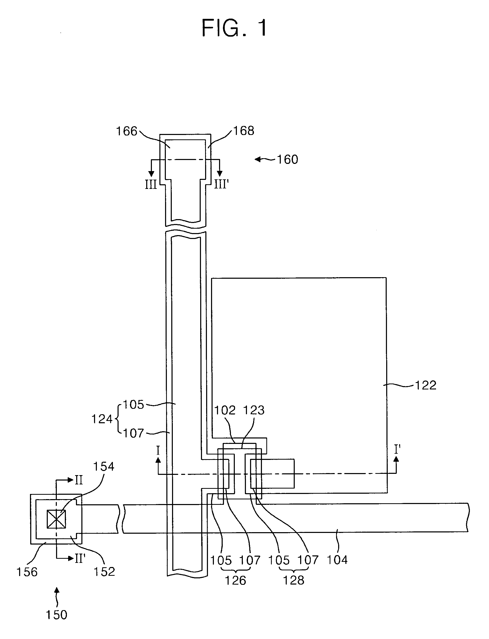
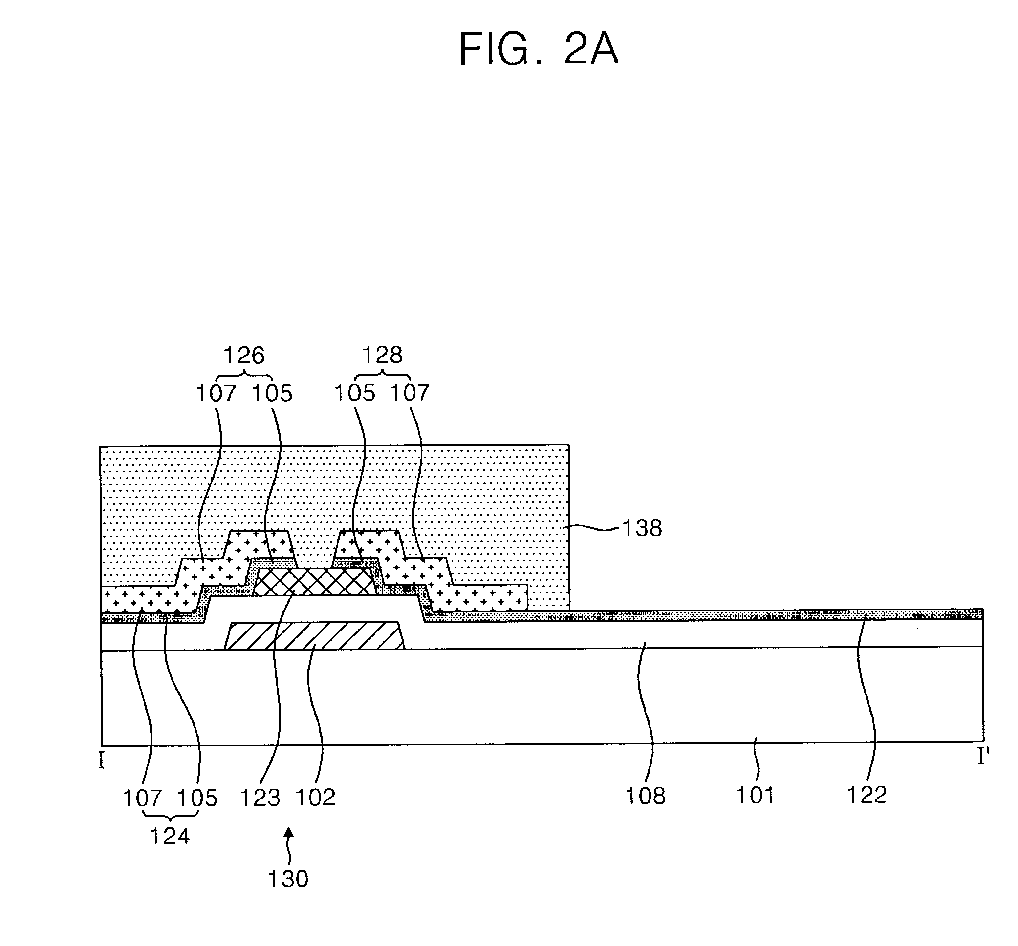
[0026]FIG. 1 is a plan view of a TFT substrate according to an embodiment of the present invention, and FIGS. 2A, 2B, and 2C are cross-sectional views of the TFT substrate taken along lines I-I′, II-II′, and III-III′, respectively of FIG. 1.

[0027]Referring to FIGS. 1, 2A, 2B, and 2C, a TFT substrate according to an embodiment of the present i...


PUM

PropertyMeasurementUnit
insulatingaaaaaaaaaa
conductiveaaaaaaaaaa
transparentaaaaaaaaaa

Abstract

A thin film transistor substrate and a method of manufacturing the same are disclosed. The method of manufacturing a thin film transistor substrate includes forming a first conductive pattern group including a gate line, a gate electrode, and a lower gate pad electrode on a substrate, forming a gate insulating layer on the substrate on which the first conductive pattern group is formed, forming an oxide semiconductor pattern overlapping the gate electrode on the gate insulating layer, and forming first and second conductive layers on the substrate on which the oxide semiconductor pattern is formed and patterning the first and second conductive layers to form a second conductive pattern group including a data line, a source electrode, a drain electrode, and a data pad.

Description

CROSS REFERENCE TO RELATED APPLICATIONS[0001]This application claims priority under 35 U.S.C. §119 to Korean Patent Application No. 10-2006-0127671 filed on Dec. 14, 2006 in the Korean Intellectual Property Office, the contents of which are herein incorporated by reference in their entirety.BACKGROUND OF THE INVENTION[0002]1. Field of the Invention[0003]The present invention relates to a thin film transistor, a thin film transistor substrate and a simplified method of manufacturing the same, which provides a liquid crystal display device having high resolution.[0004]2. Description of the Related Art[0005]A liquid crystal display (“LCD”) device displays an image by adjusting optical transmittance of liquid crystals having dielectric anisotropy by using an electric field. The LCD device includes an LCD panel having the liquid crystals aligned in a form of an active matrix and a driving circuit for driving the LCD panel.[0006]The LCD panel includes a color filter substrate and a thin f...

Claims


Application Information

Patent Timeline
Patent Type & Authority Patents(United States)
IPC IPC(8): H01L21/84H01L29/786
CPCH01L27/1214H01L29/7869H01L27/124H01L27/1225H01L29/45H01L27/1288G02F1/1339G02F1/134309G02F1/136286
Inventor LEE, EUN-GUKKIM, DO-HYUNJEONG, CHANG-OHLEE, JE-HUNLIM, SOON-KWON
Owner SAMSUNG DISPLAY CO LTD
Why Eureka
Try Eureka